background image

4

KDL-46BX427

KDL-46BX427

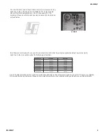
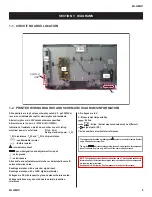
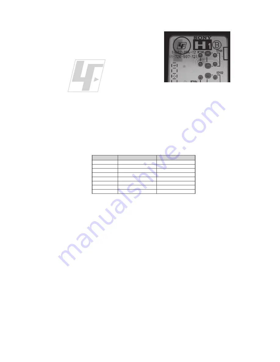
The circuit boards used in these models have been processed using 
Lead Free Solder. The boards are identified by the LF logo located 
close to the board designation e.g. H1 etc [ see example ]. The 
servicing of these boards requires special precautions to be taken as 
outlined below. 

example

It is strongly recommended to use Lead Free Solder material in order to guarantee optimal quality of new solder joints.  
Lead Free Solder is available under the following part numbers : 

Due to the higher melting point of Lead Free Solder the soldering iron tip temperature needs to be set to 370 degrees centigrade.  
This requires soldering equipment capable of accurate temperature control coupled with a good heat recovery characteristics. 

7

0

7

0

7

0

7

0

7

0

7

1

7

1

7

1

Содержание KDL-46BX427

Страница 1: ...9 883 858 51 KDL 46BX427 RM YD066 COLUMBIA LEVEL 3 CONFIDENTIAL HISTORY INFORMATION FOR THE FOLLOWING MANUAL CONFIDENTIAL ELECTRICAL SERVICE MANUAL INTERNAL ONLY ORIGINAL MANUAL ISSUE DATE 4 2011 REVISION DATE SUBJECT 4 27 2011 No revisions or updates are applicable at this time ...

Страница 2: ...agram Page 5 of 18 14 A Board Schematic Diagram Page 6 of 18 15 A Board Schematic Diagram Page 7 of 18 16 A Board Schematic Diagram Page 8 of 18 17 A Board Schematic Diagram Page 9 of 18 18 A Board Schematic Diagram Page 10 of 18 19 A Board Schematic Diagram Page 11 of 18 20 A Board Schematic Diagram Page 12 of 18 21 A Board Schematic Diagram Page 13 of 18 22 A Board Schematic Diagram Page 14 of 1...

Страница 3: ...ts Ú do not leave the module in high temperatures or in areas of high humidity for an extended period of time Ú do not expose the LCD panel to direct sunlight Ú avoid contact with water It may cause a short circuit within the module Ú disconnect the AC adapter when replacing the backlight CCFL or inverter circuit High voltage occurs at the inverter circuit at 650Vrms Ú always clean the LCD panel w...

Страница 4: ...lder is available under the following part numbers Due to the higher melting point of Lead Free Solder the soldering iron tip temperature needs to be set to 370 degrees centigrade This requires soldering equipment capable of accurate temperature control coupled with a good heat recovery characteristics r e b m u n t r a P r e t e m a i D s k r a m e R 9 1 5 0 0 0 4 6 7 m m 3 0 g K 5 2 0 0 2 5 0 0 ...

Страница 5: ...es Leakage current can be measured by any one of three methods 1 A commercial leakage tester such as the Simpson 229 or RCA WT 540A Follow the manufacturers instructions to use these instructions 2 A battery operated AC milliampmeter The Data Precision 245 digital multimeter is suitable for this job 3 Measuring the voltage drop across a resistor by means of a VOM or battery operated AC voltmeter T...

Страница 6: ...ve characteristic curve B unless otherwise noted Readings are taken with a color bar signal input Readings are taken with a 10MΩ digital multimeter Voltages are DC with respect to ground unless otherwise noted Voltage variations may be noted due to normal production tolerances All voltages are in V S Measurement impossibility B line B line Actual measured value may be different signal path RF Circ...

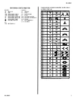
Страница 7: ...hode Common Cathode Cathode Common Common Common Common Cathode Anode Base Emitter Collector Base Emitter Collector Drain Gate Gate Drain Device Printed symbol Terminal name Circuit Terminal name of semiconductors in silk screen printed circuit Anode Anode Anode Cathode Anode Anode Cathode Transistor FET Transistor FET Emitter Collector Base Transistor Source Gate Drain Cathode Anode Anode Cathode...

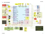
Страница 8: ...8 KDL 46BX427 KDL 46BX427 1 3 BLOCK DIAGRAM ...

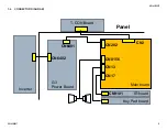
Страница 9: ...9 KDL 46BX427 KDL 46BX427 1 4 CONNECTOR DIAGRAM T CON Board Panel CN2 CN202 CN8156 CN13 CN17 CN9101 IR board Key Pad board CN6401 G3 Power Board Inverter CN6402 Main board ...

Страница 10: ...DL 46BX427 KDL 46BX427 A BOARD SCHEMATIC DIAGRAM PAGE 1 OF 18 1 5 SCHEMATICS AND SUPPORTING INFORMATION A 1 18 DC CONVERTER I 1 857 593 11 AZ2EK A P1 1 2 3 4 5 6 7 8 9 10 11 12 13 14 15 A B C D E F G H I J ...

Страница 11: ...11 KDL 46BX427 KDL 46BX427 A BOARD SCHEMATIC DIAGRAM PAGE 2 OF 18 1 2 3 4 5 6 7 8 9 10 11 12 13 14 15 A B C D E F G H I J A 2 18 DC CONVERTER II 1 857 903 11 AZ2EK A P2 ...

Страница 12: ...12 KDL 46BX427 KDL 46BX427 A BOARD SCHEMATIC DIAGRAM PAGE 3 OF 18 1 2 3 4 5 6 7 8 9 10 11 12 13 14 15 A B C D E F G H I J A 3 18 INPUT ANALOG VIDEO 1 857 903 11 AZ2EK A P3 ...

Страница 13: ...13 KDL 46BX427 KDL 46BX427 A BOARD SCHEMATIC DIAGRAM PAGE 4 OF 18 1 2 3 4 5 6 7 8 9 10 11 12 13 14 15 A B C D E F G H I J A 4 16 INPUT ANALOG VIDEO SCART 1 857 903 11 AZ2EK A P4 ...

Страница 14: ...14 KDL 46BX427 KDL 46BX427 A BOARD SCHEMATIC DIAGRAM PAGE 5 OF 18 1 2 3 4 5 6 7 8 9 10 11 12 13 14 15 A B C D E F G H I J A 5 18 INPUT ANALOG VIDEO D SUB 1 857 903 11 AZ2EK A P5 ...

Страница 15: ...15 KDL 46BX427 KDL 46BX427 A BOARD SCHEMATIC DIAGRAM PAGE 6 OF 18 1 2 3 4 5 6 7 8 9 10 11 12 13 14 15 A B C D E F G H I J A 6 18 INPUT HDMI 1 857 903 11 AZ2EK A P6 ...

Страница 16: ...16 KDL 46BX427 KDL 46BX427 A BOARD SCHEMATIC DIAGRAM PAGE 7 OF 18 1 2 3 4 5 6 7 8 9 10 11 12 13 14 15 A B C D E F G H I J A 7 18 INPUT TUNER 1 857 903 11 AZ2EK A P7 ...

Страница 17: ...17 KDL 46BX427 KDL 46BX427 A BOARD SCHEMATIC DIAGRAM PAGE 8 OF 18 1 2 3 4 5 6 7 8 9 10 11 12 13 14 15 A B C D E F G H I J A 8 18 DVB DMOD MT5135 1 857 903 11 AZ2EK A P8 ...

Страница 18: ...18 KDL 46BX427 KDL 46BX427 A BOARD SCHEMATIC DIAGRAM PAGE 9 OF 18 1 2 3 4 5 6 7 8 9 10 11 12 13 14 15 A B C D E F G H I J A 9 18 MT5366 DDR II 1 857 903 11 AZ2EK A P9 ...

Страница 19: ...19 KDL 46BX427 KDL 46BX427 A BOARD SCHEMATIC DIAGRAM PAGE 10 OF 18 1 2 3 4 5 6 7 8 9 10 11 12 13 14 15 A B C D E F G H I J A 10 18 MT5366 PERIPHERAL FLASH 1 857 903 11 AZ2EK A P10 ...

Страница 20: ...20 KDL 46BX427 KDL 46BX427 A BOARD SCHEMATIC DIAGRAM PAGE 11 OF 18 1 2 3 4 5 6 7 8 9 10 11 12 13 14 15 A B C D E F G H I J A 11 18 MT5366 HDMI INPUT_SW 1 857 903 11 AZ2EK A P11 ...

Страница 21: ...21 KDL 46BX427 KDL 46BX427 A BOARD SCHEMATIC DIAGRAM PAGE 12 OF 18 1 2 3 4 5 6 7 8 9 10 11 12 13 14 15 A B C D E F G H I J A 12 18 MT5366 LVDS OUT 1 857 903 11 AZ2EK A P12 ...

Страница 22: ...22 KDL 46BX427 KDL 46BX427 A BOARD SCHEMATIC DIAGRAM PAGE 13 OF 18 1 2 3 4 5 6 7 8 9 10 11 12 13 14 15 A B C D E F G H I J A 13 18 MT5366 GPIO INTERNAL CI 1 857 903 11 AZ2EK A P13 ...

Страница 23: ...23 KDL 46BX427 KDL 46BX427 A BOARD SCHEMATIC DIAGRAM PAGE 14 OF 18 1 2 3 4 5 6 7 8 9 10 11 12 13 14 15 A B C D E F G H I J A 14 18 MT5366 A V INTERFACE 1 857 903 11 AZ2EK A P14 ...

Страница 24: ...24 KDL 46BX427 KDL 46BX427 A BOARD SCHEMATIC DIAGRAM PAGE 15 OF 18 1 2 3 4 5 6 7 8 9 10 11 12 13 14 15 A B C D E F G H I J A 15 18 INPUT PC COMP CVBS AUDIO 1 857 903 11 AZ2EK A P15 ...

Страница 25: ...25 KDL 46BX427 KDL 46BX427 A BOARD SCHEMATIC DIAGRAM PAGE16 OF 18 1 2 3 4 5 6 7 8 9 10 11 12 13 14 15 A B C D E F G H I J A 16 18 OUTPUT SC SPDIF LR HP AUDIO 1 857 903 11 AZ2EK A P16 ...

Страница 26: ...26 KDL 46BX427 KDL 46BX427 A BOARD SCHEMATIC DIAGRAM PAGE 17 OF 18 1 2 3 4 5 6 7 8 9 10 11 12 13 14 15 A B C D E F G H I J A 17 18 AUDIO AMP 1 857 903 11 AZ2EK A P17 ...

Страница 27: ...27 KDL 46BX427 KDL 46BX427 A BOARD SCHEMATIC DIAGRAM PAGE 18 OF 18 1 2 3 4 5 6 7 8 9 10 11 12 13 14 15 A B C D E F G H I J A 18 18 IR USB KEYPAD 1 857 903 11 AZ2EK A P18 ...

Страница 28: ...T ANALOG VIDEO INPUT ANALOG VIDEO SCART INPUT ANALOG VIDEO D SUB INPUT HDMI INPUT TUNER DVB DMOD MT5135 MT5366 DDRII MT5366 PERIPHERAL FLASH MT5366 HDMI INPUT_SW MT5366 LVDS OUT MT5366 GPIO INTERNAL CI MT5366 A V INTERFACE INPUT PC COMP CVBS AUDIO OUTPUT SC SPDIF LR HP AUDIO AUDIO AMP IR USB KEYPAD COMPONENT SIDE CONDUCTOR SIDE ...

Страница 29: ...1M R6306 C6304 0 01 25V C6316 XX JL6359 C6318 XX JL6360 C6332 0 1 16V C6401 XX C6402 0 1 25V C6410 0 1 16V 10k R6215 2 2k R6402 4 7k R6404 5 6k 1 4W R6410 L6401 3 3uH L6402 3 3uH L6201 3 3uH IC6301 CXA3810M T6 1 PFC_OUT1 2 MODE1 3 AC_DETIN 4 AC_VRMS 5 PFC_ZCD 6 PFC_CS 7 PFC_VAO 8 PFC_VSENSE 9 PFC_OVP 10 PFC_TONMAX 11 RM_OFFADJ 12 RM_FMIN 13 RM_SS 14 RM_CS2 15 RM_CS1 16 RM_RT 17 VREF 18 GND 19 VCC ...

Страница 30: ... 6 2 0 4 C 6 2 0 3 C 6 2 0 1 R 6 3 5 2 R 6 3 5 1 R 6 3 5 0 R 6 3 4 9 R 6 3 4 6 R 6 3 4 5 R 6 3 4 4 R 6 3 4 3 R 6 3 4 2 R 6 3 4 0 R 6 3 3 9 R 6 3 3 7 R 6 3 3 6 R 6 3 3 5 R 6 3 3 4 R 6 3 3 3 R 6 3 3 2 R 6 3 3 1 R 6 3 3 0 R 6 3 2 5 R 6 3 2 4 R 6 3 2 2 D 6 3 2 0 R 6 3 1 8 R 6 3 1 7 R 6 3 1 6 R 6 3 1 5 D 6 3 1 9 R 6 3 1 4 D 6 3 1 8 R 6 3 1 3 D 6 3 1 7 R 6 3 1 2 D 6 3 1 6 R 6 3 1 1 D 6 3 1 5 C 6 3 3 9 R...

Страница 31: ...0R0402 PAD 1 GP R9110 0R0402 PAD 1 GP 1 2 R9127 0R0402 PAD 1 GP R9127 0R0402 PAD 1 GP 1 2 CN9101 JWT CON12 6 GP CN9101 JWT CON12 6 GP 1 2 3 4 5 6 7 8 9 10 11 12 13 14 C9110 SCD1U25V2ZY 1GP NC C9110 SCD1U25V2ZY 1GP NC 1 2 R9126 0R0402 PAD 1 GP R9126 0R0402 PAD 1 GP 1 2 C9119 SC10U10V5KX 2GP C9119 SC10U10V5KX 2GP 1 2 TP07 TP07 1 C9113 SC10U10V5KX 2GP C9113 SC10U10V5KX 2GP 1 2 C9109 SCD1U25V2ZY 1GP N...

Страница 32: ...32 KDL 46BX427 KDL 46BX427 H IR LED H BOARD PWB S NOT AVAILABLE 1 2 3 4 5 A B C D E ...

Страница 33: ...TE The components identified by shading and mark are critical for safety Replace only with part number specified NOTE The components identified by a red outline and a mark contain confidential information Specific instructions must be adhered to whenever these components are repaired and or replaced See Appendix A Encryption Key Components in the back of this manual SECTION 2 ELECTRICAL PARTS LIST...

Страница 34: ...taining encryption key components shall be identified with a red outline and a 2 Only repair boards or components listed in the service manual shall be utilized for replacement and or repair 3 Disassembly decryption or reverse engineering component s is strictly prohibited 4 Any board in which the Servicer replaces an encryption key component must be placed back into the set it orignally came from...

Отзывы: