


ICD-UX71/UX71F/UX81/UX81F/UX91F
27
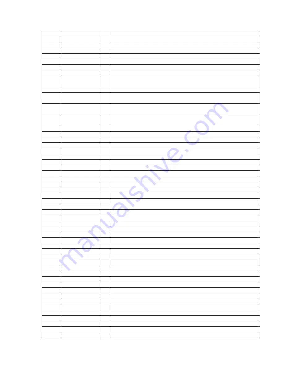
Pin No.
Pin Name
I/O
Description
P2
SCK1(P14)
O
Serial interface 1 clock signal output ADDA serial clock signal output
M4
SDO1(P15)
O
Serial interface 1 data signal output ADDA serial data signal output
L5
SDI1(P16)
I
Serial interface 1 data signal input ADDA serial data signal input
R1
TXD1(P2A)
O
UART1 transmission signal output SP/HP change signal output
T1
RXD1(P2B)
O
UART1 reception signal output SP shut down signal output
T2
TCLKA(P17)
O
Multiple timer external clock A signal output CPU core voltage change signal output
R3
TCLKB(P18)
O
Multiple timer external clock B signal output Battery level measure signal output
T3
TIOCA0(P19)
I/O
Multiple timer input capture/output compare A0 signal input/output
Not used in this set. (Open)
R4
Vdd1
—
Digital power supply pin (+1.0V)
R2
TIOCB0(P1A)
I/O
Multiple timer input capture/output compare B0 signal input/output
D AMP output on/off select signal output
P3
TIOCA1(P1B)
I/O
Multiple timer input capture/output compare A1 signal input/output
OP LED (red) signal output
P4
TIOCB1(P1C)
I/O
Multiple timer input capture/output compare B1 signal input/output
OP LED (green) signal output
R5
TXDO(P1D)
O
UART transmission signal output
T4
RXDO(P1E)
I
UART reception signal output
N4
PO0
I/O
Port pin 0 bit0 CPU power on signal output
P5
PO1
I/O
Port pin 0 bit1 Connect to ground in this set.
R6
PO2
I/O
Port pin 0 bit2 AUDIO power on signal output
T5
PO3
I/O
Port pin 0 bit3 FM power on signal output
N5
PO4
I/O
Port pin 0 bit4 Charge on signal output
M5
PO5
I/O
Port pin 0 bit5 Charge measurement signal output
M6
XFCE2(P06)
O
Nand
fl
ash chip enable 2 signal output LCD reset signal output
T6
XFCE3(P07)
O
Nand
fl
ash chip enable 3 signal output Mute signal output
P6
Vdd1
—
Digital power supply pin (+1.0V)
N6
Vss
—
Digital ground pin
R7
Vdd2
—
Digital power supply pin (+3.1V)
M7
XFWE
O
Nand
fl
ash write enable signal output
N7
XFRE
O
Nand
fl
ash read enable signal output
T7
XALE
O
Nand
fl
ash address latch enable signal output
P7
XCLE
O
Nand
fl
ash command latch enable signal output
T8
XFCE1(P1F)
O
Nand
fl
ash chip enable 1 signal output
R8
XFCE0
O
Nand
fl
ash chip enable 0 signal output
M8
XFWP
O
Nand
fl
ash write protect signal output
N8
XFBSY
I
Nand
fl
ash busy signal input
P8
FD0
I/O
Nand
fl
ash data bit 0 signal input/output
R9
FD1
I/O
Nand
fl
ash data bit 1 signal input/output
T9
FD2
I/O
Nand
fl
ash data bit 2 signal input/output
P9
FD3
I/O
Nand
fl
ash data bit 3 signal input/output
N9
FD4
I/O
Nand
fl
ash data bit 4 signal input/output
M9
FD5
I/O
Nand
fl
ash data bit 5 signal input/output
T10
FD6
I/O
Nand
fl
ash data bit 6 signal input/output
R10
FD7
I/O
Nand
fl
ash data bit 7 signal input/output
P10
Vdd1
—
Digital power supply pin (+1.0V)
N10
Vss
—
Digital ground pin
M10
Vdd2
—
Digital power supply pin (+3.1V)
N11
SDWP
I
SD card write protect signal input Connected to ground in this set.
T11
SDCD
I
SD card detect signal input Connected to ground in this set.
R11
SDCMD
I/O
SD card command signal input/output Connected to ground in this set.
P11
SDCLK
O
SD card clock signal output Not used in this set. (Open)
M11
SDAT1
I/O
SD card data bit 0 signal input/output Connected to ground in this set.
T12
SDAT2
I/O
SD card data bit 1 signal input/output Connected to ground in this set.
Содержание ICD-UX71F - Digital Flash Voice Recorder
Страница 41: ...MEMO ICD UX71 UX71F UX81 UX81F UX91F 41 ...


