


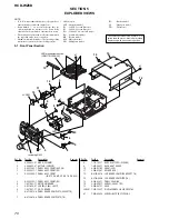


65
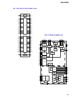
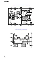
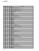
HCD-WZ8D
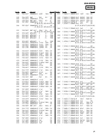
Pin No.
201
202
203
204
205
206
207
208
I/O
I
I
I/O
—
—
I/O
I/O
—
Pin Name
TCK
RESET
BUS CLK
GND
VDD
HA3
HA2
GNDP
Description
TCK signal input
ZIVA reset input
Not used
Ground terminal (inside core)
Power supply terminal (+1.8V)(inside core)
Address bus 3
Address bus 2
Ground terminal (I/O signal)