background image

DVP-C600D

4-1

4-2

SECTION  4

PRINTED  WIRING  BOARDS

AND

SCHEMATIC  DIAGRAMS

THIS NOTE IS COMMON FOR PRINTED WIRING
BOARDS AND SCHEMATIC DIAGRAMS.
(In addition to this, the necessary mote is printed
in each block.)

For printed wiring boards:

X

: indicates a lead wire mounted on the component

side.

x

: indicates a lead wire mounted on the printed side.

®

: Through hole.

p

: Parts mounted on the conductor side.

b

: Pattern from the side which enables seeing.

b

: Pattern on the rear side.

*

Circled numbers refer to waveforms.

For schematic Diagram:

Caution when replacing chip parts.
New parts must be attached after removal of chip.
Be careful not to heat the minus side of tantalum capacitor,
because it is damaged by the heat.

All resistors are in  ohms,  

1

/

4


W (Chip resistors : 

1

/

10


W)

unless otherwise specified.
k

 : 1000

, M

 : 1000k

.

All capacitors are in µF unless otherwise noted.

pF :

µµF

50V or less are not indicated except for electrolytics and
tantalums.

All variable and adjustable resistors have characteristic curve
B, unless otherwise noted.

2

: nonflammable resistor.

5

: fusible resistor.

C

: panel designation.

¢

: internal component.

C

: adjustment for repair.

*

A

: B+ Line.

*

B

: B– Line.

*

J

: IN/OUT direction of B line (+, –).

*

Circled numbers refer to waveforms.

*

Voltages are dc between measurement point.

*

Readings are taken with a color-bar signals on DVD refer-
ence disc and when plying CD reference disc.

*

Readings are taken with a digital multimeter (DC 10M

).

*

Voltage variations may be noted due to normal production
tolerances.

*

*

: indicated by the color red.

Note: The components identified by mark 

!

 or dotted line

with mark 

!

 are critical for safety.

Replace only with part number specified.

Caution:
Pattern face side:

Parts on the pattern face side seen from

(Conductor Side)

the pattern face are indicated.

Parts face side:

Parts on the parts face side seen from

(Component Side)

the parts face are indicated.

When indicating parts by reference
number, please include the board
name.

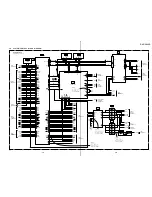
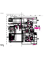
4-1. FRAME  SCHEMATIC  DIAGRAM (1/2)

FRAME (1/2)

Содержание DVP-C600D - 5 Disc Cd/dvd Player

Страница 1: ...MICROFILM SERVICE MANUAL US Model Canadian Model Mexican Model CD DVD PLAYER DVP C600D RMT D104A SPECIFICATIONS ...

Страница 2: ...ES SCHÉMATIQUES ET LA LISTE DES PIÈCES SONT CRITIQUES POUR LA SÉCURITÉ DE FONCTIONNEMENT NE REMPLACER CES COM POSANTS QUE PAR DES PIÈCES SONY DONT LES NUMÉROS SONT DONNÉS DANS CE MANUEL OU DANS LES SUPPLÉMENTS PUBLIÉS PAR SONY 1 Check the area of your repair for unsoldered or poorly sol dered connections Check the entire board surface for solder splashes and bridges 2 Check the interboard wiring t...

Страница 3: ...ic Diagram 4 39 MB 83 IF µ com Schematic Diagram 4 41 MB 83 L Gate Array Schematic Diagram 4 43 MB 83 ARP Decrypt Schematic Diagram 4 45 MB 83 System µ com Schematic Diagram 4 47 MB 83 S Gate Array Schematic Diagram 4 49 AU 198 Printed Wiring Board 4 51 AU 198 Audio 1 Schematic Diagram 4 55 AU 198 Audio 2 Schematic Diagram 4 57 AU 198 Audio 3 Schematic Diagram 4 59 AU 198 Video Buffer Schematic Di...

Страница 4: ... Table ass y Page 2 2 Chassis ass y Page 2 2 BU holder ass y Page 2 3 Rotary motor ass y Page 2 2 Loading motor ass y Page 2 2 Skew motor ass y Page 2 3 Sled motor ass y Page 2 3 Spindle motor ass y Page 2 4 TK 48 board Page 2 3 Spindle base Page 2 3 Optical pick up Page 2 4 Front panel section Page 2 1 Rear panel Page 2 1 ...

Страница 5: ...FF 1 Insert a flat blade screwdriver into a hole at the bottom and rotate the cam gear in direction A See Fig 2 Fig 2 4 HOW TO SERVICE MB 83 BOARD 1 Remove the case from the set Refer to 2 1 2 Remove the MB 83 board Refer to 2 3 3 Set the MB 83 board as shown in Fig 3 Note Do not disconnect wiring Fig 3 Case Two tapping screws Three tapping screws Two tapping screws Table Hole Cam gear A ...

Страница 6: ... MD block ass y 3 90 º with the side down confirm that the optical pick up 4 falls by self weight See Fig 5 4 Further with the front side of MD block ass y 3 up confirm that the optical pick up falls by self weight Fig 5 A 1 Sled motor ass y 2 Two screws M1 7 2 5 Upper Upper Front side Front side Lower Lower 3 MD block ass y 4 Optical pick up ...

Страница 7: ...parts the short lands have been soldered to protect from static electricity Accordingly remove solders when replacing opti cal pick up See Fig 6 Fig 6 Flexible board 3 In handling the KHS 180A RP do not touch inhibited parts shown in Fig 7 but grip the slide base bearing and U shaped guide Fig 7 KHS 180A RP Touch inhibited parts Objective lens Skew sensor Laser holder Laser coupler Flexible board ...

Страница 8: ...insulators deformed See Fig 9 7 3 Note on Mounting FG 44 Board 1 Align two bosses See Fig 10 2 Fix the board securely with screws PTPWH2 5 The sen sor will not function normally if the board floats up 7 4 Note on connecting OPT Harness 1 The optical pick up could be destroyed unless the OPT har ness is connected normally to the connector See Fig 11 Spindle motor Turn table Fig 8 Fig 9 Two step scr...

Страница 9: ...ig 13 6 Mount the lock lever See Fig 14 7 Mount the spring lock lever See Fig 14 8 Rotate the gear main in the direction of the arrow A by 90 turn Gear U D is up position See Fig 15 9 Mount the Gear rev See Fig 15 10 Fix three stopper washers on the groove of shafts See Fig 15 Gear U D Fig 12 Fig 14 Fig 13 Fig 15 Spring lock lever Spring lock lever Lock lever Lock lever Gear main Gear main Set lev...

Страница 10: ...1 1 SECTION 1 GENERAL This section is extracted from US model instruction manual DVP C600D ...

Страница 11: ...1 2 ...

Страница 12: ...1 3 ...

Страница 13: ...1 4 ...

Страница 14: ...1 5 ...

Страница 15: ...1 6 ...

Страница 16: ...1 7 ...

Страница 17: ...1 8 ...

Страница 18: ...1 9 ...

Страница 19: ...1 10 ...

Страница 20: ...1 11 ...

Страница 21: ...1 12 ...

Страница 22: ...1 13 1 13 E ...

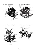
Страница 23: ... 3 Rotate the cam gear in the direction of the arrow A 0 Lug Claw Front panel section Claw Two Claws Two screws B3 9 Screw B3 5 Tray cover ass y 8 Screw B3 4 Draw out the table A 6 Four claws 7 Tray guard 9 Four flat wires CN101 302 452 252 2 Three flat wires CN301 601 701 3 Flat wire CN251 6 Two screws B3 5 Three screws B3 4 Connector CN361 1 Two connectors CN001 002 0 Cover lower 7 Cover upper 8...

Страница 24: ...wo screws B3 2 Two brackets guide B1 4 Two brackets guide B1 3 Two screws B3 5 Table ass y 4 Two screws B3 7 Two screws B2 6 3 1 Tapping screw M3 12 5 Bracket RM ass y 6 Belt RM 2 Table rotary 3 Connector CN701 8 Rotary motor ass y 1 Four screws B3 2 Four screws B3 3 Chassis ass y 4 Screw B3 5 Loading motor ass y 1 Belt timing 3 Harness 2 Connector ...

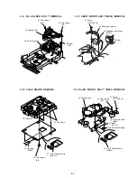
Страница 25: ...screws B3 4 Screw B3 3 Bracket CP 5 BU holder ass y 3 Two screws B3 4 Two claws 2 OP 15 flexible board CN001 1 Flat wire CN002 TK 48 board 2 Claw 3 Skewgear retainer 4 Skewgear motor ass y M902 1 Screw PTTWH2 5 3 Skew shaft stopper 7 Sled motor ass y M501 5 Screw PTTWH2 5 4 Spindle base 1 OP 15 flexible board CN001 2 Screw P2 8 6 Two screws P1 7 2 5 ...

Страница 26: ...Flat wire CN002 4 Optical pick up 3 Main shaft 2 Screw PTTWH2 5 1 OP 15 flexible board CN001 Skew motor ass y M902 X 3947 138 1 Sled motor ass y M501 X 3947 137 1 Optical pick up KHS 180A J1N 8 820 005 02 DC motor spindle M901 1 763 131 11 Sled motor ass y M501 X 3947 137 1 Optical pick up KHS 180A J1N 8 820 005 02 DC motor spindle 1 763 131 11 ...

Страница 27: ...AUDIO FG 44 SLED POWER BLOCK HS 934SU POWER SUPPLY CK 78 CONNECTION SE 70 SENSOR LM 55 LOADING MOTOR LE 20 LED HP 97 HEAD PHONE FR 134 FUNCTION SWITCH MB 83 SIGNAL PROCESS DC MOTOR SPINDLE TK 48 RF SERVO FL 89 FL DRIVER FUNCTION SWITCH 2 5 E ...

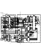
Страница 28: ...ATE ARRAY IC802 1M SRAM YC0 7 IC804 2 2 L GATE ARRAY IC801 EEPROM IC803 8M ROM IC806 ARP IC810 4M DRAM IC203 AV DECODER IC201 202 16M SRAM IC104 AC 3 DECODER IC105 256K SRAM SPDIF IC102 DIR IC101 M GATE ARRAY AV_DATA AV_BLK AV_LRCK IC215 AUDIO 2CH DAC IC851 VIDEO BUFFER IC351 VIDEO BUFFER IC203 205 DAC IC208 213 5 1OUTPUT AUDIO 1 2 AUDIO IN PHONE COMPNENT VIDEO OUT MEGA CONTROL VIDEO 1 2 S VIDEO 1...

Страница 29: ...IN OUT IN2 OUT2 IN1 OUT1 IC506 SERVO DSP IC508 FILTER IC501 COMP 3 1 6 7 10 8 12 14 21 24 26 11 12 8 73 99 IC503 9 20 6 23 3 1 GIO11 2 88 7 1 49 46 26 IC502 2 2 11 12 5 10 7 8 13 14 15 16 17 18 23 22 19 8 9 27 7 10 11 30 31 14 15 32 33 34 1 28 29 75 14 74 41 38 8 12 13 18 25 32 2 5 33 34 29 30 22 23 Q371 MUTE Q372 MUTE IC363 IC303 IC301 SPINDLE MOTOR DRIVE IC302 SLED MOTOR DRIVE 19 20 3 5 65 79 3 ...

Страница 30: ... AVCS AVINT AVWT MRST RF SERVO SEE PAGE 3 3 4 SYSTEM CONTROL SEE PAGE 3 9 10 IA0 7 ID0 7 IA0 8 ID0 7 SD0 7 SD0 7 DCRSD0 7 AREQ ALALID ERROR TOS DTI0 7 DTO0 7 SDCK XSHD XSRO XSAK SDEF CD_LRCK CD_BCK CD_DATA SPDIF 54 51 28 111 105 106 107 SYSTEM CONTROL SEE PAGE 3 9 10 CGCSO CS IC201 16M SDRAM AVA0 11 AVID 0 15 IC202 16M SDRAM SDQM WE CAS RAS CS1 CS2 SDQM SDCLK A_0 8 D_0 7 21 24 26 30 98 99 101 102 ...

Страница 31: ... 8 Y C Q351 INVERTER CN252 CN201 CN851 CN251 VIDEO_V VIDEO Y VIDEO C B Y Y R Y V MUTE V MUTE VS Q352 VS AU 198 BOARD 1 3 SEE PAGE 4 61 MB 83 BOARD 3 6 SEE PAGE 4 23 YOUT COUT CPOUT Y G OUT R Y B OUT FID V SYNC H SYNC PD0 7 B Y R OUT SIGNAL PROCESS SEE PAGE 3 6 SYSTEM CONTROL SEE PAGE 3 9 10 MODE CONTROL SEE PAGE 3 13 19 ı 22 24 ı 27 MRST VCS 13 5M AVCK SOG2 VSI 27M_VE MRST VCS 4 13 7 10 2 15 1 C Y...

Страница 32: ...4 47 4 11 13 14 16 21 MLT MLT 31 ı 33 SDSPRD SDSPWR BUSY2 ERROR LDOUT LDIN NST CD DVD SDEN SPCTRL1 DVDLDON CDLDON TILT H SSSD SCKG3 SCKG3 SOG3 D2LT SPCTRL0 SPGC2 SPGC1 S12VOFF TBLL TBLR S1 S3 TSENS DSENS FON S12VOFF SDSPRD SDSPWR BUSY2 ERROR LDOUT LDIN NST CD DVD AVWT AVCS DCRWT DCRINT DCRCS IWR IRD ARPWT ARPCS ARPINT MUTE MD2 DFCT NORF LOCK FWON OHSYNC XIFBSY IFSI IFSO DIAG XSHINT AVWT AVCS DCRWT...

Страница 33: ...DIO_MUTE SCKG3 D2LT SOG3 SPDIF DAC_LRCK DAC_BCK DAC_ADATA DD_LCK DD_BCK 384FS 2CH MRST DD_DATAF DD_DATAR DD_DATAC 384FS_DAC GAIN6 SCKG4 SOG4 DDLT1 DDLT2 DDLT3 6 9 7 8 5 3 1 2 4 6 HP_L HP_R PMUTE 10 22 21 20 22 7 F F R C R C 9 25 18 5 3 1 19 10 17 15 13 12 11 IC101 M GATE ARRAY IC001 Q002 MUTE Q001 MUTE HP AMP PHONES J001 IC352 IC215 IC203 IC204 IC205 CENTER WOOFER DAC SURROUND DAC FRONT L R DAC GA...

Страница 34: ...SHUFFLE S406 TIME TEXT S405 DISPLAY S404 DISC 3 S403 DISC 2 S402 DISC 1 S122 EX CHANGE S120 DISC 5 S101 DISC 4 IC605 RESET IC606 S LINK COMP MEGA CONTROL J351 J352 S LINK IC 101 FL DRIVER IC401 REMOTE CONTROL RECEIVER ON STANDBY D401 INPUT JOG MEGA CONTROL D102 D101 D108 IC603 IC604 I F µ COM IC601 ROM ALE OE WE A00 019 AD00 07 LATCH S119 OPEN CLOSE S118 PLAY S108 PREV S107 STOP S106 PAUSE S110 JO...

Страница 35: ...01 VCC OPTICAL DEVAICE S 5V IC004 IC005 IC006 IC011 24 25 1 2 7 8 6 4 8 9 14 5 3 1 5 6 AU 9V AU 9V IC011 2 1 17 9 22 21 23 1 CN601 IC601 IC602 IC603 IC604 IC605 IC606 IC608 IC204 IC205 IC206 IC207 IC209 IC252 IC101 IC812 LPF Q001 002 SWITCH IC801 IC803 IC804 IC805 IC807 IC811 IC802 IC301 IC452 IC455 IC501 IC502 IC503 IC506 IC507 IC508 IC363 F001 IC361 F002 IC302 IC303 F003 F004 S12V OFF SYSTEM CON...

Страница 36: ... indicated except for electrolytics and tantalums All variable and adjustable resistors have characteristic curve B unless otherwise noted 2 nonflammable resistor 5 fusible resistor C panel designation internal component C adjustment for repair A B Line B B Line J IN OUT direction of B line Circled numbers refer to waveforms Voltages are dc between measurement point Readings are taken with a color...

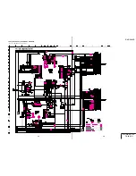
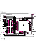
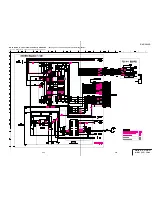
Страница 37: ...DVP C600D 4 3 4 4 FRAME 2 2 FRAME SCHEMATIC DIAGRAM 2 2 ...

Страница 38: ...RF SERVO PRINTED WIRING BOARD Ref No TK 48 board 3 000 series There are few cases that the part isn t mounted in this model is printed on this diagram RF SERVO TK 48 AU 198 AUDIO FG 44 SLED POWER BLOCK HS 934SU POWER SUPPLY CK 78 CONNECTION SE 70 SENSOR LM 55 LOADING MOTOR LE 20 LED HP 97 HEAD PHONE FR 134 FUNCTION SWITCH MB 83 SIGNAL PROCESS DC MOTOR SPINDLE TK 48 RF SERVO FL 89 FL DRIVER FUNCTIO...

Страница 39: ... 800 mVp p V 4 IC005 CD play 500 mV DIV 1 ms DIV 5 IC005 CD play 500 mV DIV 10 ms DIV 6 IC005 CD play 500 mV DIV 1 µs DIV Note The components identi fied by mark or dotted line with mark are criti cal for safety Replace only with part number specified Note Les composants identifiés par une marque sont critiques pour la sécurité Ne les remplacer que par une piéce portant le numéro spécifié ...

Страница 40: ...DVP C600D 4 9 4 10 TK 48 RF SERVO 2 SCHEMATIC DIAGRAM Ref No TK 48 board 3 000 series RF SERVO 2 TK 48 2 2 ...

Страница 41: ... 6 IC604 E 7 IC608 E 7 IC701 D 7 IC803 F 4 IC804 E 6 IC805 E 3 IC806 B 4 Q371 C 3 Q372 C 4 Q501 A 5 Q701 D 8 There are few cases that the part isn t mounted in this model is printed on this diagram SIGNAL PROCESS MB 83 AU 198 AUDIO FG 44 SLED POWER BLOCK HS 934SU POWER SUPPLY CK 78 CONNECTION SE 70 SENSOR LM 55 LOADING MOTOR LE 20 LED HP 97 HEAD PHONE FR 134 FUNCTION SWITCH MB 83 SIGNAL PROCESS DC...

Страница 42: ... F 2 IC101 B 1 IC105 C 1 IC201 C 7 IC202 D 8 IC204 B 6 IC207 B 7 IC208 C 7 IC209 D 2 IC302 B 2 IC361 C 2 IC363 C 5 IC452 A 4 IC502 B 2 IC503 B 2 IC507 C 4 IC601 F 2 IC602 F 3 IC605 E 2 IC606 F 1 IC801 E 3 IC802 F 4 IC807 F 6 IC810 B 5 IC811 D 7 IC812 B 6 Q001 E 7 Q002 E 7 Q452 C 5 Q601 E 1 Q602 E 1 R533 R417 C274 C203 R203 MB 83 BOARD SIDE B A B C D E 05 F 1 2 3 4 1 617 019 5 6 7 8 11 ...

Страница 43: ...DVP C600D 4 15 4 16 MB 83 AC 3 DECODER SCHEMATIC DIAGRAM See page 4 11 to 4 14 for printed wiring board Ref No MB 83 board 2 000 series AC 3 DECODER MB 83 1 16 ...

Страница 44: ...DVP C600D 4 17 4 18 MB 83 M GATE ARRAY SCHEMATIC DIAGRAM See page 4 11 to 4 14 for printed wiring board Ref No MB 83 board 2 000 series M GATE ARRAY MB 83 2 16 ...

Страница 45: ...DVP C600D 4 19 4 20 MB 83 AV DECODER SCHEMATIC DIAGRAM See page 4 11 to 4 14 for printed wiring board Ref No MB 83 board 2 000 series AV DECODER MB 83 3 16 ...

Страница 46: ...1 4 22 MB 83 CLOCK GENERATOR SCHEMATIC DIAGRAM See page 4 11 to 4 14 for printed wiring board Ref No MB 83 board 2 000 series CLOCK GENERATOR MB 83 4 16 Waveforms 1 IC206 8 3 28 Vp p 27 MHz 2 IC209 1 1 4 Vp p 27 MHz ...

Страница 47: ...DVP C600D 4 23 4 24 MB 83 VIDEO ENCODER SCHEMATIC DIAGRAM See page 4 11 to 4 14 for printed wiring board Ref No MB 83 board 2 000 series VIDEO ENCODER MB 83 5 16 ...

Страница 48: ...1 000 series There are few cases that the part isn t mounted in this model is printed on this diagram SLED FG 44 AU 198 AUDIO FG 44 SLED POWER BLOCK HS 934SU POWER SUPPLY CK 78 CONNECTION SE 70 SENSOR LM 55 LOADING MOTOR LE 20 LED HP 97 HEAD PHONE FR 134 FUNCTION SWITCH MB 83 SIGNAL PROCESS DC MOTOR SPINDLE TK 48 RF SERVO FL 89 FL DRIVER FUNCTION SWITCH 1 669 310 11 11 05 FG 44 BOARD ...

Страница 49: ...6 Waveforms 1 IC303 ª DVD play 5 2 Vp p 160 Hz 2 IC303 ª CD play 1 84 Vp p 45 Hz Note The components identi fied by mark or dotted line with mark are criti cal for safety Replace only with part number specified Note Les composants identifiés par une marque sont critiques pour la sécurité Ne les remplacer que par une piéce portant le numéro spécifié ...

Страница 50: ... C600D 4 29 4 30 DRIVE 2 SLED MB 83 7 16 FG 44 MB 83 DRIVE 2 FG 44 SLED SCHEMATIC DIAGRAMS See page 4 11 to 4 14 and 4 26 for printed wiring boards Ref No MB 83 board 2 000 series FG 44 board 1 000 series ...

Страница 51: ...DVP C600D 4 31 4 32 MB 83 DSP 1 SCHEMATIC DIAGRAM See page 4 11 to 4 14 for printed wiring board Ref No MB 83 board 2 000 series DSP 1 MB 83 8 16 ...

Страница 52: ...DVP C600D 4 33 4 34 Waveform 1 IC506 3 6 Vp p 27 MHz MB 83 DSP 2 SCHEMATIC DIAGRAM See page 4 11 to 4 14 for printed wiring board Ref No MB 83 board 2 000 series DSP 2 MB 83 9 16 ...

Страница 53: ...ING MOTOR SENSOR MB 83 10 16 CK 78 LM 55 SE 70 MB 83 ROULETTE CK 78 CONNECTION LM 55 LOADING MOTOR SE 70 SENSOR SCHEMATIC DIAGRAM See page 4 11 to 4 14 for printed wiring board Ref No MB 83 board 2 000 series CK 78 LM 55 SE 70 boards 1 000 series ...

Страница 54: ...K 78 LM 55 SE 70 4 37 4 38 AU 198 AUDIO FG 44 SLED POWER BLOCK HS 934SU POWER SUPPLY CK 78 CONNECTION SE 70 SENSOR LM 55 LOADING MOTOR LE 20 LED HP 97 HEAD PHONE FR 134 FUNCTION SWITCH MB 83 SIGNAL PROCESS DC MOTOR SPINDLE TK 48 RF SERVO FL 89 FL DRIVER FUNCTION SWITCH 1 669 319 11 11 05 SE 70 BOARD CK 78 BOARD 05 1 669 324 11 11 LM 55 BOARD 1 669 326 11 11 05 ...

Страница 55: ... 000 series 4 39 4 40 Note The components identi fied by mark or dotted line with mark are criti cal for safety Replace only with part number specified Note Les composants identifiés par une marque sont critiques pour la sécurité Ne les remplacer que par une piéce portant le numéro spécifié BIAS MB 78 11 16 ...

Страница 56: ...DVP C600D 4 41 4 42 MB 83 IF µ COM SCHEMATIC DIAGRAM See page 4 11 to 4 14 for printed wiring board Ref No MB 83 board 2 000 series IF µ COM MB 83 12 16 Waveform 1 IC604 5 6 Vp p 4 MHz ...

Страница 57: ... 3 3 Vp p 27 MHz 3 IC806 0 1 5 Vp p 4 IC806 3 0 Vp p 33 MHz 5 IC806 3 4 Vp p 27 MHz 6 IC811 3 4 Vp p 27 MHz L GATE ARRAY MB 83 13 16 MB 83 L GATE ARRAY SCHEMATIC DIAGRAM See page 4 11 to 4 14 for printed wiring board Ref No MB 83 board 2 000 series 4 43 4 44 ...

Страница 58: ...DVP C600D 4 45 4 46 ARP DECRYPT MB 83 14 16 MB 83 ARP DECRYPT SCHEMATIC DIAGRAM See page 4 11 to 4 14 for printed wiring board Ref No MB 83 board 2 000 series ...

Страница 59: ...DVP C600D MB 83 SYSTEM µ COM SCHEMATIC DIAGRAM See page 4 11 to 4 14 for printed wiring board Ref No MB 83 board 2 000 series SYSTEM µ COM MB 83 15 16 4 47 4 48 ...

Страница 60: ...DVP C600D 4 49 4 50 S GATE ARRAY MB 83 16 16 MB 83 S GATE ARRAY SCHEMATIC DIAGRAM See page 4 11 to 4 14 for printed wiring board Ref No MB 83 board 2 000 series Waveform 1 IC805 4 4 Vp p 20 MHz ...

Страница 61: ...209 B 5 IC210 B 6 IC211 A 4 IC212 A 5 IC213 A 6 IC214 C 11 IC215 B 7 IC217 C 7 IC301 B 2 IC351 B 10 IC353 B 3 IC851 B 1 Q201 B 8 Q202 A 8 Q205 B 8 Q207 A 4 Q208 A 4 Q209 A 5 Q210 A 5 Q211 A 6 Q212 A 6 Q352 B 9 AU 198 AUDIO FG 44 SLED POWER BLOCK HS 934SU POWER SUPPLY CK 78 CONNECTION SE 70 SENSOR LM 55 LOADING MOTOR LE 20 LED HP 97 HEAD PHONE FR 134 FUNCTION SWITCH MB 83 SIGNAL PROCESS DC MOTOR SP...

Страница 62: ...361 A 3 D362 C 2 D363 C 4 D364 A 4 IC352 A 3 Q206 B 4 Q213 C 10 Q214 B 10 Q215 B 10 Q216 C 5 Q351 B 3 Q353 A 2 Q354 A 1 4 53 4 54 A B C 1 2 3 4 5 6 7 8 9 10 11 05 AU 198 BOARD SIDE A 1 669 319 11 11 MEGA CONTROL S LINK DIGITAL OUT COAXIAL DIGITAL OUT OPTICAL S VIDEO OUT LINE OUT 5 1CH OUTPUT AUDIO IN COMPONENT VIDEO OUT ...

Страница 63: ...DVP C600D 4 55 4 56 AUDIO 1 AU 198 1 4 AU 198 AUDIO 1 SCHEMATIC DIAGRAM See page 4 51 to 4 54 for printed wiring board Ref No AU 198 board 1 000 series ...

Страница 64: ...DVP C600D 4 57 4 58 AUDIO 2 AU 198 2 4 AU 198 AUDIO 2 SCHEMATIC DIAGRAM See page 4 51 to 4 54 for printed wiring board Ref No AU 198 board 1 000 series ...

Страница 65: ...DVP C600D 4 59 4 60 AUDIO 3 AU 198 3 4 AU 198 AUDIO 3 SCHEMATIC DIAGRAM See page 4 51 to 4 54 for printed wiring board Ref No AU 198 board 1 000 series ...

Страница 66: ...RAM See page 4 51 to 4 54 for printed wiring board Ref No AU 198 board 1 000 series 4 61 4 62 VIDEO BUFFER AU 198 4 4 Waveforms 1 IC351 1 1 Vp p H 2 IC351 1 0 Vp p H 3 IC351 0 0 7 Vp p H 4 IC851 0 7 Vp p H 5 IC851 0 7 Vp p H 6 IC851 0 1 0 Vp p H ...

Страница 67: ...R FUNCTION SW LED FL 89 LE 20 There are few cases that the part isn t mounted in this model is printed on this diagram FL 89 BOARD SIDE B CN102 D 1 D101 D 13 D102 C 11 D104 D 9 D106 D 9 D108 C 11 D109 C 11 D110 D 11 D111 C 11 D112 C 11 D113 C 9 FL 89 BOARD SIDE A CN101 B 6 CN103 A 13 D103 A 10 IC101 C 5 Q101 D 9 Q102 D 9 Q103 D 13 Q104 D 11 Q105 C 11 Q106 A 12 AU 198 AUDIO FG 44 SLED POWER BLOCK H...

Страница 68: ...DVP C600D 4 65 4 66 FL 89 FL DRIVER FUNCTION SWITCH LE 20 LED SCHEMATIC DIAGRAMS Ref No FL 89 LE 20 board 1 000 series FL DRIVER FUNCTION SW LED FL 89 LE 20 ...

Страница 69: ...iagram AU 198 AUDIO FG 44 SLED POWER BLOCK HS 934SU POWER SUPPLY CK 78 CONNECTION SE 70 SENSOR LM 55 LOADING MOTOR LE 20 LED HP 97 HEAD PHONE FR 134 FUNCTION SWITCH MB 83 SIGNAL PROCESS DC MOTOR SPINDLE TK 48 RF SERVO FL 89 FL DRIVER FUNCTION SWITCH FR 134 BOARD POWER ON STANDBY DISC 1 DISPLAY DISC 2 DISC 3 TIME TEXT SHUFFLE 1 669 321 11 11 05 HP 97 BOARD SIDE A 1 669 321 11 11 05 HP 97 BOARD SIDE...

Страница 70: ...DVP C600D FR 134 FUNCTION SWITCH HP 97 HEAD PHONE SCHEMATIC DIAGRAMS Ref No FR 134 HP 97 boards 1 000 series FUNCTION SW HEAD PHONE FR 134 HP 97 4 69 4 70 ...

Страница 71: ...11 B 4 D611 C 4 IC301 D 4 IC511 B 5 IC611 A 4 Q101 C 3 Q102 D 3 Q103 B 3 Q211 B 5 Q311 C 5 Q312 D 5 Q511 B 5 Q512 B 5 There are few cases that the part isn t mounted in this model is printed on this diagram AU 198 AUDIO FG 44 SLED POWER BLOCK HS 934SU POWER SUPPLY CK 78 CONNECTION SE 70 SENSOR LM 55 LOADING MOTOR LE 20 LED HP 97 HEAD PHONE FR 134 FUNCTION SWITCH MB 83 SIGNAL PROCESS DC MOTOR SPIND...

Страница 72: ... GND AU 12V 10V GND MTR 12V MTR GND R306 1 5K R305 220 R304 1 5K C512 47µF 35V C511 1000µF 25V L511 10µH 2 6A L311 10µH 2 6A L211 10µH 2 6A C513 47µF 35V C514 47µF 35V R512 10K P511 60V 750mA Q511 2SK2279 12V REG R511 10K C311 330µF 35V C312 330µF 35V C313 47µF 35V C611 560µF 35V D212 RD24EB2 24V 1W IC611 PQ3RD13 I O G CT C211 330µF 35V C212 47µF 35V R211 10K R212 10K Q211 2SJ488 P211 60V 750mA P3...

Страница 73: ...ress and data set 93 100 A8 15 I O Set address 5 1 INTERFACE CONTROL PIN FUNCTION IC604 on MB 83 Board 12 16 Pin No Pin Name I O Function Pin No Pin Name I O Function 1 4 A16 19 I O Set Address 5 6 TIN0 1 Not used 7 8 TOT0 1 Not used 9 ALE O Output of address latch enablesignal 10 OE O Output of output enablesignal 11 GND GND 12 WRL O Output of write enablesignal 13 WRH Not used 14 HRQ Not used 15...

Страница 74: ... O Output of A mute signal 65 PA11 O Output of MA mute signal 66 IRQ0 I Input of interrupt fromIC203 67 IRQ1 I Input of DMA request from IC203 68 IRQ2 I Input of V SYNC FID interrupt signal 69 IRQ3 I Input of interrupt from IC804 70 VCC Digital power supply 71 CK O Output of internal clock 72 VSS Digital ground 73 EXTAL 20MHz crystal connection pin 74 XTAL 20MHz crystal connection pin 75 VCC Digit...

Страница 75: ...t used 105 PB7 Not used 106 VSS Digital ground 107 RxD0 I Input of serial data 108 TxD0 O Output of serial data 109 RxD1 I Input of serial data 110 TxD1 O Output of serial data 111 SCK0 O Output of serial clock 112 SCK1 O Output of serial clock Pin No Pin Name I O Function ...

Страница 76: ...eck As item No is 2 2 enter 0202 Syscon Diagnosis IF con Ver 0 620 9315 SYScon Ver 0 400 0000 Select Diag No 0 Enter item No 0 Press Remocon Key SIRCS FF KEY FF Figure 3 Syscon Diagnosis IF con Ver 0 620 9315 SYScon Ver 0 400 0000 Select Sub No 02 Enter item No 02 Press Remocon Key SIRCS FF KEY FF Figure 4 Syscon Diagnosis IF con Ver 0 620 9315 SYScon Ver 0 400 0000 Select Sub No 02 0 Enter item N...

Страница 77: ...external RAM IC802 are checked twice by inverting the data but in the simple check one block is checked then the subsequent 4 blocks are skipped and also a check of in verted data is not executed If write read mismatch error occurred checking can be repeated 3 Destination Setting 3 2 Destination setting Check I O port read Error Not detected The destination setting port I O is read and displayed w...

Страница 78: ... is initialized by the reset is checked First the version No is read then its comple ment is written After hardware reset the data is read again and if it matches the written data the reset error occurs 6 Data Source 6 2 Register in ARP IC806 Register write Register read matching check Error 05 Write read data mismatch error Data from 0x00 up to 0xff are written to 12 registers where all bits can ...

Страница 79: ...ters where all bits can be written read then they are read to check for matching If write read mismatch error occurred checking can be repeated 7 3 Reset Line in 64020 Register write Hard reset Register read matching check Error 02 Reset error 05 Write read data mismatch error After 0xff is written to the Capture Compare Control Register 0 whether it is initialized to 0x00 by the reset pulse signa...

Страница 80: ... be 12 times exactly but 1 errors are allowable 8 5 Still Picture Output SDRAM IC201 202 direct write Pattern data AV Decoder IC203 Video Out Error 31 AV Decoder IC203 interruption DMA transfer is not detected The pattern is directly written to the SDRAM IC201 202 in AV Decoder IC203 then its picture display is checked First the brightness signal data are written by the amount of one screen while ...

Страница 81: ... is displayed to prompt for key entry Analog outputs are muted 9 6 Audio Digital Mute ROM audio data ARP IC806 AV Decoder IC203 Digi tal Audio I F output Error 10 ARP IC806 AV Decoder IC203 data transfer error 37 PLL DAC IC209 serial transfer interruption is not de tected AC 3 audio bit stream data stored in ROM IC803 are transferred to the AV Decoder IC203 via ARP IC806 and output to the Digital ...

Страница 82: ...as in MPEG Audio Analog Output but the sound level in the second check will be very lowered about 48dB If no error is found the message is displayed to prompt for key entry 9 11 MGA DCS Select Switch Check ROM audio data ARP IC806 AV Decoder IC203 MGA Analog audio output Error 10 ARP IC806 AV Decoder IC203 data transfer error 35 2ch DAC IC215 serial transfer interruption is not de tected 37 PLL DA...

Страница 83: ...d left and right surrounding channels respectively us ing the MGA If no error is found the message is displayed to prompt for key entry 10 7 AC 3 Audio Output ROM audio data ARP IC806 AV Decoder IC203 DIR IC102 AC 3 DSP AC 3 DAC IC203 205 Audio signal output Error 10 ARP IC806 AV Decoder IC203 data transfer error 35 2ch DAC IC215 serial transfer interruption is not de tected 37 PLL DAC IC209 seria...

Страница 84: ...nterruption is not detected 33 SSI interruption is not detected 34 DNR interruption is not detected 35 2ch DAC interruption is not detected 36 EEPROM interruption is not detected 37 PLL DAC interruption is not detected 40 1914 ID error 41 Vsync interruption is not detected 42 Vsync interrupt cycle error 43 AC 3 DAC for main interruption is not detected 44 AC 3 DAC for center interruption is not de...

Страница 85: ... 8 If All is selected the screen shown in Figure 9 is displayed Drive Auto Adjustment SA 00000 SI 00 EMG OO 0 Adjustment ALL 0 All 2 CD 2 DVD SL 3 DVD DL START Press ENTER Key Blinking STOP Press STOP Key Figure 9 The tray opens after the ENTER key is pressed and the initial ization is finished Then place the disc for adjustment If ALL is selected place three discs DVD_SL CD and DVD_DL for ad just...

Страница 86: ...ing ON Sled ON AGC ON CLVA Lock Check Auto Filter Offset Auto Focus Offset Auto Tilt Offset Auto Focus Offset servo stop Go To Home Position LD ON Spindle start Tilt ON Focus ON FOK Check Tan Position FOK Check Tracking ON Sled ON AGC ON CLVA Tangential skew adjustment 10k tj RVS 3 STOP STOP STOP STOP Open Place a disc or three discs Identify the disc NG OK NG OK NG OK NG OK NG OK NG OK NO YES OK ...

Страница 87: ... close chuck Go To Home Position Disc Type Check NG NO OK LD ON Spindle start Tilt ON Focus ON 4 STOP STOP 2 5 Tracking ON Sled ON CLVA Auto Tracking Offset FOK Check STOP NG OK Lock Check STOP NG OK Auto Focus Offset Auto Focus Gain Auto Tracking Gain Pull in Memory Jitter Check Servo STOP Search Check STOP NG OK OK Select ALL or DVD_DL NO YES close chuck Go To Home Position 6 7 8 5 CD adjustment...

Страница 88: ...Tilt Offset Auto Focus Offset Auto Focus Gain Auto Tracking Gain Auto EQ Layer Check Jitter Check STOP STOP NG OK NG Focus Jump L0 n L1 9 FOK Check Tracking ON Sled ON CLVA Layer Check STOP STOP NG OK NG OK DVD_DL adjustment Auto Focus Offset Auto Focus Gain Auto Tracking Gain Auto EQ Pull in Memory OPEN 8 OK STOP close chucking Go To Home Position Tan Position Message to apply a drop of locking a...

Страница 89: ...owing points Select correct disc type on the Disc Type screen First select 0 Disc TYpe and execute 7 Hydet init and 8 Sled init See Figure 12 In case of abnormality press STOP immediately to stop opera tion and turn off the power Do not execute Auto Adjust while executing FG Pause Also as these commands are not protected take care not to press wrong key When PLL is locked the sector address or tim...

Страница 90: ...500TJ Jump 500 tracks reversely fine search 4 FWD 10KTJ Jump 10k tracks forward direct search 5 RVS 10KTJ Jump 10k tracks reversely direct search 6 FJ0 1 After layer jump L0 L1 tracking loop does not turn on 7 FJ1 0 After layer jump L1 L0 tracking loop does not turn on 8 LJ0 1 After layer jump L0 L1 tracking loop turns on 9 LJ1 0 After layer jump L1 L0 tracking loop turns on FWD 1TJ Jump one track...

Страница 91: ...s after focus offset and tangential skew are adjusted 2 Auto Focus Offset Adjust focus offset automatically Adjusted result is reflected on the EEPROM Execute this with CLVA turned on If NG retry this after tilt offset and tangential skew are ad justed 30 3 Auto Focus Gain Adjust focus gain automatically Adjusted result is reflected on the EEPROM Execute this with CLVA turned on if possible If NG ...

Страница 92: ... are effective SD About 50 E0 HY About 60 A0 6 7 Other Operation For manual operation of the drive the following operations are available besides the operations given on the menu screen Com mon to front panel and remote commander Eject Loading OPEN CLOSE Stop Open and button Close Chuck Clear CLEAR button Movement throughout the menu Stop STOP button Servo stop Retrun RETURN button Return to drive...

Страница 93: ...ry With the initial menu displayed press 4 key on the standard com mander and the information on emergency history of Drvcon and Syscon will be displayed This information is given over four pages which can be changed over with and keys To return to the initial menu press RETURN key EMG Hist Page 1 CD 000000 Hour 1 00 00 00 00 00 00 00 00 00 00 00 00 2 00 00 00 00 00 00 00 00 00 00 00 00 Page Down ...

Страница 94: ...At the mode change command the mode could not be changed within specified time and the drive stopped A2 Retry due to supply error failed and the drive stopped A3 Disc directory configuration and information file are illegal and the drive stopped A4 The drive stopped as a DVD R disc was used A5 Coded data could not be decoded and the drive stooped A6 At slow R the destination of reverse search is i...

Страница 95: ...e digit service number combination of a letter and figures flashes on the screen and front panel display 1 Each user needs to manage the error C code C 13 ππ The disc is dirty Clean the disc with a cleaning cloth C 31 ππ The disc is not inserted correctly Open the disc tray and insert the disc correctly MECHA MODE is shown in ππ position Code Description 00 Power ON Ready 10 Stop 20 Trace data sup...

Страница 96: ...mode change command the mode could not be changed within specified time and the drive stopped A2 Retry due to supply error failed and the drive stopped A3 Disc directory configuration and information file are illegal and the drive stopped A4 The drive stopped as a DVD R disc was used A5 Coded data could not be decoded and the drive stooped A6 At slow R the destination of reverse search is illegal ...

Страница 97: ... satisfies the specification SECTION 7 ELECTRICAL ADJUSTMENT DVP C600D In making adjustment refer to 7 4 Adjustment Related Parts Arrangement Note During diagnostic check the characters and color bars can be seen only with the NTSC monitor Therefore for diag nostic check use the monitor that supports both NTSC and PAL modes This section describes procedures and instructions necessary for adjusting...

Страница 98: ...u 0 Syscon Diagnosis set so that CXD1914 color bars are generated 2 Adjust the RV251 to attain 1 0 02 Vp p Figure 7 2 2 S terminal Output Check MB 83 board Purpose Check S terminal video output If it is incorrect pictures will not be displayed correctly in spite of connection to the TV with an S terminal cable Mode CXD1914 ENC check in test mode menu 0 Syscon Diagnosis Signal Color bars Test point...

Страница 99: ... it is not correct the colors will be too dark or light Mode CXD1914 ENC check in test mode menu 0 Syscon Diagnosis Signal Color bars Test point CN252 pin Instrument Oscilloscope Specification 286 20 mVp p Connection Checking method 1 Confirm that the S C burst is 286 20 mVp p Figure 7 7 7 Checking S Video Output DC Level MB 83 board Purpose This checks signals for S1 and S2 compatible TV If they ...

Страница 100: ...éro spécifié Ref No Part No Description Remark Ref No Part No Description Remark 12 A 6065 127 A AU 198 BOARD COMPLETE 13 1 783 344 11 CABLE FLAT FMA 5 25P 14 4 957 280 31 BRACKET GUIDE B1 15 1 468 288 11 POWER BLOCK HS 934SU 16 3 957 819 01 FOOT 17 3 051 059 01 PLATE BOTTOM 18 3 654 748 01 SPACER 19 3 051 301 01 SPRING SHIELD 20 1 475 686 61 COMMANDER STANDARD RMT D104A 21 3 709 044 01 LID BATTER...

Страница 101: ...B VOLUME Ref No Part No Description Remark Ref No Part No Description Remark 64 3 950 989 01 NUT M7 HEXAGON 65 3 051 077 01 BRACKET HP 66 4 951 620 01 SCREW 2 6X8 BVTP 67 A 6065 123 A HP 97 BOARD COMPLETE 68 A 6065 122 A FR 134 BOARD COMPLETE 69 3 051 079 01 REINFORCEMENT 70 1 783 346 11 CABLE FLAT FML 6 20P 71 A 6065 121 A FL 89 BOARD COMPLETE 72 A 6065 124 A LE 20 BOARD COMPLETE 73 1 475 685 11 ...

Страница 102: ...SCREW PTPWH 2 6X20 109 X 4943 480 1 BRACKET ROLLER D ASSY 110 3 970 608 11 SUMITITE B3 BV 111 4 957 278 01 BEARING ROTARY A 112 X 3948 858 1 GEAR ROTARY ASSY 113 3 051 076 01 BELT RM 114 X 3948 857 1 BRACKET RM ASSY 115 3 051 083 01 TABLE ROTARY 116 3 051 063 01 GEAR DRIVE 117 3 325 697 01 WASHER 118 1 783 352 11 CABLE FLAT FSC 6 12P 119 A 6065 129 A SE 70 BOARD COMPLETE M951 A 6062 080 A MOTOR AS...

Страница 103: ...57 288 01 GEAR MAIN 165 4 957 283 01 WASHER 5 STOPPER 166 4 957 287 01 GEAR REV 167 4 957 286 01 GEAR U D 168 3 051 074 01 BRACKET CP 169 3 051 062 01 PULLEY CHUCKING 170 3 051 082 01 STOPPER BU 171 4 981 923 01 SCREW M STEP 172 1 783 342 11 CABLE FLAT FMF 29 8P 173 A 6065 125 A TK 48 BOARD COMPLETE 174 1 783 340 11 CABLE FLAT FMT 22 27P 175 3 051 073 01 HOLDER BU 176 A 6065 130 A CK 78 BOARD COMP...

Страница 104: ...R SKEW GEAR 214 3 975 057 01 GEAR SKEW 215 4 974 711 01 SCREW 2X5 P TYIGHT PTTWH 216 4 974 725 01 SCREW M1 7X2 5 P 218 A 4683 008 A GEAR ASSY LIMITTER 219 4 974 720 01 GEAR S B M501 X 3947 137 1 MOTOR ASSY SLED M901 1 763 131 11 MOTOR DC SPINDLE M903 X 3947 138 1 MOTOR ASSY SKEW TILT 8 1 5 DVD MECHANISM DECK ASSEMBLY 207 206 215 208 209 215 210 219 218 220 216 211 215 215 205 204 202 202 203 202 2...

Страница 105: ...LECT 10uF 20 50V C232 1 136 850 11 FILM 0 1uF 5 63V C233 1 163 021 91 CERAMIC CHIP 0 01uF 10 50V C234 1 130 467 00 MYLAR 470PF 5 50V C235 1 126 926 11 ELECT 1000uF 20 10V C236 1 130 467 00 MYLAR 470PF 5 50V C237 1 104 664 11 ELECT 47uF 20 16V C238 1 104 664 11 ELECT 47uF 20 16V C239 1 124 910 11 ELECT 47uF 20 50V C240 1 124 910 11 ELECT 47uF 20 50V C241 1 104 664 11 ELECT 47uF 20 16V C242 1 104 66...

Страница 106: ...D D363 8 719 975 40 DIODE RB411D D364 8 719 016 73 DIODE STZ6 8TT146 FERRITE BEAD FB201 1 414 553 11 FERRITE 0UH FB202 1 414 553 11 FERRITE 0UH FB203 1 414 553 11 FERRITE 0UH FB204 1 414 553 11 FERRITE 0UH FB205 1 414 553 11 FERRITE 0UH FB206 1 414 553 11 FERRITE 0UH FB207 1 414 553 11 FERRITE 0UH FB208 1 414 553 11 FERRITE 0UH FB209 1 414 135 11 FERRITE 0UH FB210 1 414 135 11 FERRITE 0UH FB211 1 ...

Страница 107: ...330K 5 1 10W R234 1 216 109 00 METAL CHIP 330K 5 1 10W R235 1 216 109 00 METAL CHIP 330K 5 1 10W R236 1 216 109 00 METAL CHIP 330K 5 1 10W R237 1 216 073 00 METAL CHIP 10K 5 1 10W R238 1 216 109 00 METAL CHIP 330K 5 1 10W R239 1 216 073 00 METAL CHIP 10K 5 1 10W R240 1 216 073 00 METAL CHIP 10K 5 1 10W R241 1 216 041 00 METAL CHIP 470 5 1 10W R242 1 216 041 00 METAL CHIP 470 5 1 10W R243 1 216 109...

Страница 108: ...100 5 1 10W R349 1 216 025 91 RES CHIP 100 5 1 10W R350 1 216 057 00 METAL CHIP 2 2K 5 1 10W R351 1 216 021 00 METAL CHIP 68 5 1 10W R352 1 216 021 00 METAL CHIP 68 5 1 10W R353 1 216 021 00 METAL CHIP 68 5 1 10W R354 1 216 021 00 METAL CHIP 68 5 1 10W R355 1 216 021 00 METAL CHIP 68 5 1 10W R356 1 216 021 00 METAL CHIP 68 5 1 10W R357 1 216 057 00 METAL CHIP 2 2K 5 1 10W R358 1 216 073 00 METAL C...

Страница 109: ... RESISTOR R105 1 216 037 00 METAL CHIP 330 5 1 10W R106 1 216 037 00 METAL CHIP 330 5 1 10W R108 1 216 083 00 METAL CHIP 27K 5 1 10W R109 1 216 037 00 METAL CHIP 330 5 1 10W R110 1 216 073 00 METAL CHIP 10K 5 1 10W R111 1 216 055 00 METAL CHIP 1 8K 5 1 10W R112 1 216 053 00 METAL CHIP 1 5K 5 1 10W R113 1 216 073 00 METAL CHIP 10K 5 1 10W R114 1 216 063 91 RES CHIP 3 9K 5 1 10W R115 1 216 009 00 ME...

Страница 110: ... 91 RES CHIP 3 9K 5 1 10W R408 1 216 295 91 SHORT 0 SWITCH S401 1 771 349 21 SWITCH KEYBOARD POWER S402 1 771 349 21 SWITCH KEYBOARD DISC 1 S403 1 771 349 21 SWITCH KEYBOARD DISC 2 S404 1 771 349 21 SWITCH KEYBOARD DISC 3 S405 1 771 349 21 SWITCH KEYBOARD DISPLAY S406 1 771 349 21 SWITCH KEYBOARD TIME TEXT S407 1 771 349 21 SWITCH KEYBOARD SHUFFLE A 6065 123 A HP 97 BOARD COMPLETE Ref No 1 000 Ser...

Страница 111: ...0 01uF 10 25V C208 1 162 970 11 CERAMIC CHIP 0 01uF 10 25V C209 1 162 970 11 CERAMIC CHIP 0 01uF 10 25V C210 1 162 970 11 CERAMIC CHIP 0 01uF 10 25V C211 1 162 970 11 CERAMIC CHIP 0 01uF 10 25V C214 1 162 970 11 CERAMIC CHIP 0 01uF 10 25V C215 1 162 964 11 CERAMIC CHIP 0 001uF 10 50V C216 1 162 970 11 CERAMIC CHIP 0 01uF 10 25V C217 1 162 970 11 CERAMIC CHIP 0 01uF 10 25V C218 1 162 970 11 CERAMIC...

Страница 112: ...68 1 128 004 11 ELECT CHIP 10uF 20 16V C469 1 162 970 11 CERAMIC CHIP 0 01uF 10 25V C470 1 107 826 11 CERAMIC CHIP 0 1uF 10 16V C502 1 162 964 11 CERAMIC CHIP 0 001uF 10 50V C503 1 124 778 00 ELECT CHIP 22uF 20 6 3V C504 1 107 826 11 CERAMIC CHIP 0 1uF 10 16V C506 1 162 964 11 CERAMIC CHIP 0 001uF 10 50V C507 1 162 959 11 CERAMIC CHIP 330PF 5 50V C510 1 107 826 11 CERAMIC CHIP 0 1uF 10 16V C511 1 ...

Страница 113: ... 162 970 11 CERAMIC CHIP 0 01uF 10 25V C834 1 162 970 11 CERAMIC CHIP 0 01uF 10 25V C835 1 162 970 11 CERAMIC CHIP 0 01uF 10 25V C836 1 162 970 11 CERAMIC CHIP 0 01uF 10 25V C837 1 162 970 11 CERAMIC CHIP 0 01uF 10 25V C838 1 162 970 11 CERAMIC CHIP 0 01uF 10 25V C839 1 162 970 11 CERAMIC CHIP 0 01uF 10 25V C840 1 162 970 11 CERAMIC CHIP 0 01uF 10 25V C841 1 162 970 11 CERAMIC CHIP 0 01uF 10 25V C...

Страница 114: ...3 21 FILTER CHIP EMI FL213 1 239 400 11 FILTER CHIP EMI FL214 1 239 400 11 FILTER CHIP EMI FL252 1 233 893 21 FILTER CHIP EMI FL254 1 233 893 21 FILTER CHIP EMI FL501 1 233 893 21 FILTER CHIP EMI FL502 1 233 893 21 FILTER CHIP EMI FL601 1 233 893 21 FILTER CHIP EMI FL801 1 233 893 21 FILTER CHIP EMI FL802 1 233 893 21 FILTER CHIP EMI FL803 1 233 893 21 FILTER CHIP EMI FL804 1 233 893 21 FILTER CHI...

Страница 115: ... 1 16W R106 1 216 837 11 METAL CHIP 22K 5 1 16W R107 1 216 829 11 METAL CHIP 4 7K 5 1 16W R108 1 216 829 11 METAL CHIP 4 7K 5 1 16W R109 1 216 811 11 METAL CHIP 150 5 1 16W R110 1 500 283 11 INDUCTOR CHIP 0UH R115 1 216 025 91 RES CHIP 100 5 1 10W R117 1 216 025 91 RES CHIP 100 5 1 10W R119 1 216 833 11 METAL CHIP 10K 5 1 16W R120 1 216 833 11 METAL CHIP 10K 5 1 16W R123 1 216 801 11 METAL CHIP 22...

Страница 116: ...4 11 METAL CHIP 0 5 1 16W R277 1 216 864 11 METAL CHIP 0 5 1 16W R278 1 216 864 11 METAL CHIP 0 5 1 16W R279 1 216 813 11 METAL CHIP 220 5 1 16W R280 1 216 809 11 METAL CHIP 100 5 1 16W R281 1 216 801 11 METAL CHIP 22 5 1 16W R282 1 216 801 11 METAL CHIP 22 5 1 16W R283 1 216 805 11 METAL CHIP 47 5 1 16W R284 1 216 805 11 METAL CHIP 47 5 1 16W R285 1 216 805 11 METAL CHIP 47 5 1 16W R286 1 216 827...

Страница 117: ...16W R459 1 216 864 11 METAL CHIP 0 5 1 16W R460 1 216 809 11 METAL CHIP 100 5 1 16W R486 1 216 821 11 METAL CHIP 1K 5 1 16W R487 1 216 821 11 METAL CHIP 1K 5 1 16W R488 1 216 857 11 METAL CHIP 1M 5 1 16W R489 1 216 819 11 METAL CHIP 680 5 1 16W R490 1 216 839 11 METAL CHIP 33K 5 1 16W R491 1 216 833 11 METAL CHIP 10K 5 1 16W R492 1 216 839 11 METAL CHIP 33K 5 1 16W R493 1 216 833 11 METAL CHIP 10K...

Страница 118: ... 50 1 16W R628 1 216 864 11 METAL CHIP 0 5 1 16W R630 1 216 821 11 METAL CHIP 1K 5 1 16W R631 1 216 821 11 METAL CHIP 1K 5 1 16W R632 1 216 833 11 METAL CHIP 10K 5 1 16W R633 1 216 809 11 METAL CHIP 100 5 1 16W R635 1 216 809 11 METAL CHIP 100 5 1 16W R636 1 216 821 11 METAL CHIP 1K 5 1 16W R637 1 216 833 11 METAL CHIP 10K 5 1 16W US Canadian R638 1 216 833 11 METAL CHIP 10K 5 1 16W R640 1 216 833...

Страница 119: ...R855 1 216 833 11 METAL CHIP 10K 5 1 16W R856 1 216 837 11 METAL CHIP 22K 5 1 16W R857 1 216 825 11 METAL CHIP 2 2K 5 1 16W R858 1 216 838 11 METAL CHIP 27K 5 1 16W R859 1 216 825 11 METAL CHIP 2 2K 5 1 16W R860 1 216 821 11 METAL CHIP 1K 5 1 16W R861 1 216 833 11 METAL CHIP 10K 5 1 16W R862 1 216 833 11 METAL CHIP 10K 5 1 16W R863 1 216 809 11 METAL CHIP 100 5 1 16W R864 1 216 809 11 METAL CHIP 1...

Страница 120: ...IC611 9 880 436 01 IC PQ3RD13 COIL L101 1 424 117 11 COIL CHOKE 18mH PROTECTOR P211 1 533 589 11 PROTECTOR 750mA 60V P311 1 533 593 11 PROTECTOR 2A 60V P312 1 533 589 11 PROTECTOR 750mA 60V P511 1 533 589 11 PROTECTOR 750mA 60V PHOTO COUPLER PC101 8 749 010 59 COUPLER PHOTO TLP721F TRANSISTOR Q101 9 880 437 01 TRANSISTOR 2SK2789 Q102 8 729 024 00 TRANSISTOR 2SC3377 Q103 9 880 437 01 TRANSISTOR 2SK...

Страница 121: ... C097 1 163 038 91 CERAMIC CHIP 0 1uF 25V C098 1 163 021 91 CERAMIC CHIP 0 01uF 10 50V C099 1 163 019 00 CERAMIC CHIP 0 0068uF 10 50V C100 1 163 021 91 CERAMIC CHIP 0 01uF 10 50V C101 1 163 021 91 CERAMIC CHIP 0 01uF 10 50V C102 1 163 021 91 CERAMIC CHIP 0 01uF 10 50V C103 1 163 021 91 CERAMIC CHIP 0 01uF 10 50V C104 1 126 205 11 ELECT CHIP 47uF 20 6 3V C105 1 163 021 91 CERAMIC CHIP 0 01uF 10 50V...

Страница 122: ... 356 11 CABLE FLAT FMA 6 9P 10 1 777 850 51 CORD POWER 13 1 783 344 11 CABLE FLAT FMA 5 25P 70 1 783 346 11 CABLE FLAT FML 6 20P 73 1 475 685 11 ENCODER ROTARY JOG CURSOR BUTTON 118 1 783 352 11 CABLE FLAT FSC 6 12P 163 1 466 996 11 ENCODER ROTARY LOADING 172 1 783 342 11 CABLE FLAT FMF 29 8P 174 1 783 340 11 CABLE FLAT FMT 22 27P 207 8 820 005 02 OPTICAL PICK UP KHS 180A J1N 208 1 665 390 11 OP 1...

Страница 123: ... 178 Sony Corporation Home A V Products Company 9 921 686 11 DVP C600D 98G0537 1 Printed in Japan 1998 7 Published by General Engineering Dept Osaki East ...

Отзывы: