background image

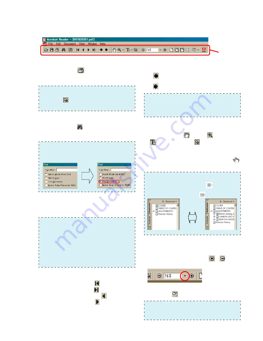
[Description of main button functions on toolbar of the Adobe Acrobat Reader Ver5.0 (for Windows)]

Printing a text

1. Click the Print button 

.

2. Specify a printer, print range, number of copies, and other op-

tions, and then click [OK].

Application of printing:

To set a range to be printed within a page, select the graphic

selection tool 

 and drag on the page to enclose a range to

be printed, and then click the Print button.

Finding a text

1. Click the Find button 

.

2. Enter a character string to be found into a text box, and click

the [Find]. (Specify the find options as necessary)

Application to the Service Manual:

To execute “find” from current page toward the previous pages,
select the check box “Find Backward” and then click the
“Find”.

3. Open the find dialog box again, and click the [Find Again] and

you can find the matched character strings displayed next.
(Character strings entered previously are displayed as they are
in the text box.)

Application to the Service Manual:

The parts on the drawing pages (block diagrams, circuit dia-
grams, printed circuit boards) and parts list pages in a text
can be found using this find function. For example, find a
Ref. No. of IC on the block diagram, and click the [Find Again]
continuously, so that you can move to the Ref. No. of IC on
the circuit diagram or printed circuit board diagram succes-
sively.

Note:

The find function may not be applied to the Service

Manual depending on the date of issue.

Switching a page

• To move to the first page, click the 

.

• To move to the last page, click the 

.

• To move to the previous page, click the 

.

• To move to the next page, click the 

.

Reversing the screens displayed once

• To reverse the previous screens (operation) one by one, click

the 

.

• To advance the reversed screens (operation) one by one, click

the 

.

Application to the Service Manual:

This function allows you to go and back between circuit dia-
gram and printed circuit board diagram, and accordingly it
will be convenient for the voltage check.

Moving with link

1. Select either palm tool 

, zoom tool 

, text selection tool

, or graphic selection tool 

.

2. Place the pointer in the position in a text where the link exists

(such as a button on cover and the table of contents page, or
blue characters on the removal flowchart page or drawing

page), and the pointer will change to the forefinger form 

.

3. Then, click the link. (You will go to the link destination.)

Moving with bookmark:

Click an item (text) on the bookmark pallet, and you can move

to the link destination. Also, clicking 

  can display the

hidden items.

(To go back to original state, click 

)

Zooming or rotating the screen display

“Zoom in/out”

• Click the triangle button in the zoom control box to select the

display magnification. Or, you may click 

 or 

 for zoom-

ing in or out.

“Rotate”

• Click rotate tool 

, and the page then rotates 90 degrees each.

Application to the Service Manual:

The printed circuit board diagram you see now can be changed
to the same direction as the set.

Toolbar

Содержание Cyber-shot DSC-P43

Страница 1: ... flexible boards harnesses are shown Ver 1 0 2004 04 DIGITAL STILL CAMERA On the CH 146 and SY 101 boards This service manual procides the information that is premised the circuit board replacement service and not intended repair inside the CH 146 and SY 101 boards Therefore schematic diagram printed wiring board and electrical parts list of the CH 146 and SY 101 boards are not shown The following...

Страница 2: ...s 71 30 91 mm 2 7 8 1 3 16 3 5 8 inches W H D Mass Approx 90 g 3 oz x AC LS5 AC Adaptor not supplied Input rating AC 100 to 240 V 50 60 Hz 11 W 0 16 to 0 09 A Output rating DC 4 2 V 1 5 A Operating temperature range 0 to 40 C 32 to 104 F Storage temperature range 20 to 60 C 4 to 140 F Dimensions Approx 48 29 81 mm 1 15 16 1 3 16 3 1 4 inches W H D protruding portions not included Mass Approx 130 g...

Страница 3: ...der melts at a temperature about 40 C higher than ordinary solder Ordinary soldering irons can be used but the iron tip has to be applied to the solder joint for a slightly longer time Soldering irons using a temperature regulator should be set to about 350 C Caution The printed pattern copper foil may peel away if the heated tip is applied for too long so be careful Strong viscosity Unleaded sold...

Страница 4: ...2 3 7 4 PRINTED WIRING BOARDS AND SCHEMATIC DIAGRAMS 4 1 Frame Schematic Diagram 4 1 4 2 Schematic Diagrams 4 5 CD 501 CCD IMAGER 4 7 SW 420 CONTROL SWITCH LCD DRIVE 4 27 ST 098 FLASH DRIVE 4 29 MS FP 861 FLEXIBLE MEMORY STICK CONNECTOR 4 31 FP 860 FLEXIBLE JACK 4 32 MICROPHONE UNIT MA 001 4 33 CONTROL SWITCH BLOCK RL51510 4 34 4 3 Printed Wiring Boards 4 35 CD 501 4 37 SW 420 4 43 ST 098 4 45 MS ...

Страница 5: ... W 1 215 869 11 Wrap insulating tape fully around the leads of the resistor to prevent electrical shock 1 kΩ 1 W Wrap insulating tape Discharging the Capacitor Short circuit between the positive and the negative terminals of charged capacitor with the short jig about 10 seconds 1 1 NOTE FOR REPAIR Make sure that the flat cable and flexible board are not cracked of bent at the terminal Do not inser...

Страница 6: ...he power off and on again Format the Memory stick Insert a new Memory Stick Cause Trouble with hardware Unformatted memory stick is inserted Memory stick is broken Caution Display During Error SYSTEM ERROR FORMAT ERROR MEMORY STICK ERROR E 61 ss E 91 ss Checking of lens drive circuit When failed in the focus and zoom initialization Abnormality when flash is being charged Checking of flash unit or ...

Страница 7: ...le CN706 3 FP 852 CN703 4 ST 098 5 Tapping screw x2 6 SP retainer plate 7 FP 860 CN751 8 FP 861 CN705 9 Tapping screw x2 0 SY 101 qa BT harness CN001 qs Tapping screw x1 qd MS 1 Mic unit flexible CN707 2 DC motor harness CN602 3 Front cabinet 1 Screw M1 7 x2 2 Microphone unit 1 Caution label 2 Tape A 3 FP 853 CN702 4 FP 856 CN601 5 Lens block 5 1 3 2 1 1 1 2 3 4 5 2 2 4 6 2 3 1 2 4 7 0 qd 5 6 5 3 ...

Страница 8: ...e board Flush unit ST 098 board MS board SY 101 board Control switch block AC power adaptor AC IN Color monitor DSC P43 only 1 2 Setting the STILL or MOVIE mode Before turn on the power you have to keep a switch SW1 pushed in order to maintain the STILL or MOVIE mode Setting the VIEW mode Before turn on the power you have to keep a switch SW2 pushed in order to maintain the VIEW mode ...

Страница 9: ... FP 861 Board Name Function CD 501 CCD IMAGER CH 146 CCD SIGNAL PROCESS included in SY 101 MS FP 861 MEMORY STICK CONNECTOR ST 098 FLASH DRIVE SW 420 CONTROL SWITCH LCD DRIVE SY 101 CAMERA MODULE CAMERA DSP LENS DRIVE SH DSP Including CH 146 FRONT CONTROL AUDIO DC DC CONVERTER FP 860 FP 859 FP 852 FP 853 Microphone unit Control switch block FP 856 ...

Страница 10: ...DSC P41 P43 HELP HELP Sheet attachment positions and procedures of processing the flexible boards harnesses are shown SY 101 board Caution label Tape A Tape A ...

Страница 11: ...ink 3 BLOCK DIAGRAMS OVERALL BLOCK DIAGRAM 2 2 POWER BLOCK DIAGRAM 2 2 POWER BLOCK DIAGRAM 1 2 OVERALL BLOCK DIAGRAM 1 2 OVERALL BLOCK DIAGRAM 2 2 POWER BLOCK DIAGRAM 2 2 POWER BLOCK DIAGRAM 1 2 OVERALL BLOCK DIAGRAM 1 2 ...

Страница 12: ...S RST MC XCS IC 302REG MC XCS IC 302SDRAM XSYS RST XPANEL TG CS XPANEL TG CS VIDEO AMP ON P1 MC CKIO A2 A6 AC12 AA9 AC16 AC15 AD19 AB11 B6 B5 G3 J2 D6 LENS TEMP VER EXT CLK PANEL B PANEL G C1 D2 39 38 SW 420 BOARD 1 2 2 6 16 32 34 35 13 12 11 23 22 16 21 19 PANEL UNIT CN752 1 2 11 XFC RST SENS LENS BARIA OUT A B AU AOUT A6 B5 A4 B4 8 6 5 17 19 20 10 9 19 15 16 7 11 21 22 19 135 37 48 29 26 2 1 8 1...

Страница 13: ... RST B3 J5 J4 D7 X401 32 768kHz RESET S251 252 254 256 258 260 FUNCTION KEY 39 38 37 36 S253 W D Zoom S257 S261 T MOVIE STILL VIEW KEY AD0 1 KEY AD2 KEY AD0 1 KEY AD2 CN201 2 2 CN752 2 2 A2 A4 AU OUT 33 A3 XAV JACK IN 29 C8 XMS IN Q401 B6 22 39 38 USB JACK IN A V OUT MONO USB DATA 2 3 1 USB CN752 J002 FP 860 FLEXIBLE BOARD 1 2 5 ı 11 12 1 2 3 4 3 1 XSHTA ON XAE LOCK ON XPWR ON XPOWER LED ON CHG SW...

Страница 14: ...CONTROLLER 5 8 ST UNREG G8 A7 ACV SENS F8 DD CON SENS BATT XEXT H8 BATT SENS F001 F003 F002 F004 9 CN706 BACK UP VCC BT001 LITHIUM BATTERY 5 ı 11 12 1 2 3 4 OUT3A J3 VCC5 DIN CLK SYSDDON USB PWR ON LD CS FCHG K5 Q009 Q006 007 Q002 Q005 D011 CN751 CN001 13 ı 19 ACV UNREG1 FP 860 FLEXIBLE BOARD DC IN J001 BT901 BATTERY TERMINAL BATT UNREG BATT GND ACV GND BATT XEXT 36 VLL 3V DC CONTROL VCH5 J5 OUT5 ...

Страница 15: ...L153 IRIS DRIVE 3 8 IC602 L301 PI006 W2 VCC 9 XLENZ RST LED ST 098 BOARD CN851 9 ı 12 T851 FLASH UNIT L701 Q703 706 Q201 202 9 ı 12 1 1 FLASH CONTROL 17 CN203 CN202 BL THH VSH 6 1 10 VDC 9 VGH SW 420 BOARD BL L 3 BL H 33 CN201 XC SAVE2 4 9V REG Q751 34 32 16 VDD 8 VDD 10 5 6 4 12 24 EXTDA 28 BACKLIGHT COLOR LCD MONITOR D901 LCD901 LCD DRIVE IC201 PANEL UNIT CH 146 BOARD CCD SIGNAL PROCESSOR TIMING...

Страница 16: ...AM_ 8 0V V1 CAM_15V GND H1B GND GND D_2 8V GND VST GND H1A GND GND V3A GND V5A GND RG EVER H2B XTALLY_LED V2 GND V3B VHOLD XCHARGE_LED GND H2A GND V5B VSUB RANDOM_TRIG V6 CCD OUT POWER_SAVE VSUB_CONT XAE_LOCK_LED V4 CAM_ 8 0V V1 CAM_15V GND H1B GND GND D_2 8V GND VST NC NC NC GSRT GPCK GRES CP VDD 3V VGH 15V VDC 15V VSS C1 C2 VGL VSS VDD 3V VSH 5V VR VB VG HCNT MCLK OE SRT 25 STBYB 26 VBC 27 VCOM ...

Страница 17: ...ARD MEMORY STICK CONNECTOR SW 420 BOARD CONTROL SWITCH LCD DRIVE CD 501 BOARD CCD IMAGER FP 860 FLEXIBLE BOARD JACK MICROPHONE UNIT MA 001 CONTROL SWITCH BLOCK RL51510 ST 098 BOARD FLASH DRIVE MS BOARD FP 861 FLEXIBLE BOARD MEMORY STICK CONNECTOR SW 420 BOARD CONTROL SWITCH LCD DRIVE CD 501 BOARD CCD IMAGER COMMON NOTE FOR SCHEMATIC DIAGRAMS COMMON NOTE FOR SCHEMATIC DIAGRAMS ...

Страница 18: ...VIDEO SIGNAL ANALOG A AUDIO SIGNAL ANALOG A VIDEO AUDIO SIGNAL A VIDEO AUDIO SERVO SIGNAL A SERVO SIGNAL Circled numbers refer to waveforms Measuring conditions voltage and waveform Voltages and waveforms are measured between the measurement points and ground when camera shoots color bar chart of pattern box They are reference values and reference waveforms VOM of DC 10 MΩ input impedance is used ...

Страница 19: ...H THE 05 G SY 101 11 PAGE 4 12 10 E 2 D CCD IMAGER CCD BLOCK 9 F 4 B C 12 3 CD 501 BOARD 5 6 REC Y CHROMA SIGNAL PATH VIDEO SIGNAL FLASH CHARGE AE AF LOCK SELE TIMER RECORDING VSUB GND VSUB_CONT GND RANDOM_TRIG POWER_SAVE GND RG GND H1B H1A GND H2B H2A GND V6 V5B V5A V4 V3B V3A V2 V1 VST VHOLD GND GND CAM_ 8 0V GND CAM_15V GND CCD OUT GND GND EVER XCHARG_LED XAE_LOCK_LED XTALLY_LED D_2 8V V6 V 5B ...

Страница 20: ...Schematic diagrams of the CH 146 and SY 101 boards are not shown Pages from 4 9 to 4 26 are not shown ...

Страница 21: ... 3300 R251 MAZW068H0LS0 D252 S260 MAZW068H0LS0 D251 S253 S261 1200 R254 S256 R261 XX S257 LND251 STATIC_GND 3300 R259 S255 1200 R253 1500 R252 3300 R258 R255 1200 1k R260 S258 1 A SI XVD XHD STBYB SRT GRES HCNT OE XVD MCLK STBYB HCNT CP GSRT XSCK XHD VCOM MCLK VCOM OE VG SI VB XCS GPCK VR SO CP GRES SO SRT GPCK XCS GSRT XSCK VB VG VR KEY_AD1 KEY_AD0 MODE_DIAL0 KEY_AD2 KEY_AD1 KEY_AD0 MODE_DIAL0 KE...

Страница 22: ...RANS DRIVE TRANS DRIVE CHARGING CAPACITOR FLASH CONTROL IC851 NC OUT VDD GND IN FLASH UNIT FLASH DRIVE FLASH DRIVE ST BLOCK F 4 10 E B C 2 7 XX MARK NO MOUNT 8 3 D 9 ST 098 BOARD 5 6 05 A_5V STB_ON XSTRB_PWRSAVE STB_FULL REG_GND REG_GND REG_GND REG_GND ST_UNREG ST_UNREG ST_UNREG ST_UNREG 4 2 SCHEMATIC DIAGRAMS ST 098 BOARD 4 2 SCHEMATIC DIAGRAMS ST 098 BOARD For Schematic Diagram Refer to page 4 4...

Страница 23: ...n FP 860 flexible board BT001 LITHIUM BATTERY SP901 SPEAKER 0 1u C001 CN001 1 2 3 4 5 6 7 8 9 10 1 A DATA1 VSS INT DIO DATA3 DATA2 VSS SCLK BS VCC STATIC_GND B 3 C 2 05 4 MEMORY STICK CONNECTOR MS BOARD FP 861 FLEXIBLE BOARD 5 6 MEMORY STICK STICK MEMORY 7 D SIGNAL SIGNAL PATH PB Y CHROMA VIDEO SIGNAL AUDIO REC 10 12 1 11 8 8 SY 101 CN705 PAGE 4 25 of LEVEL3 VSS VCC MC_MSCLK XMS_IN MC_MSD2 MC_MSD1...

Страница 24: ...SY 101 5 8 10 2 1 PAGE 4 20 of LEVEL3 MICROPHONE UNIT MA 001 is replaced as block so that PRINTED WIRING BOARD is omitted 1 A 3 B 2 4 C D 05 8 7 1 4 3 2 6 5 MICROPHONE MICROPHONE UNIT MA 001 PAGE 4 21 of LEVEL3 CN707 SY 101 6 8 MIC_GND PRELAMP_AF_ON MIC_IN REG_GND A_5V LENCV_CLOSE_SENS LENCV_OPEN_SENS N C LED SELF TIMER AF ILLUMINATOR SIGNAL PATH AUDIO REC SIGNAL SW1 LENS COVER OPEN DETECT SW2 LEN...

Страница 25: ...IBLE BOARD FP 860 FLEXIBLE BOARD CD 501 BOARD CIRCUIT BOARDS LOCATION COMMON NOTE FOR PRINTED WIRING BOARDS MOUNTED PARTS LOCATION FLEXIBLE BOARDS LOCATION CIRCUIT BOARDS LOCATION COMMON NOTE FOR PRINTED WIRING BOARDS MOUNTED PARTS LOCATION FLEXIBLE BOARDS LOCATION Board Name Function CD 501 CCD IMAGER SW 420 CONTROL SWITCH LCD DRIVE ST 098 FLASH DRIVE MS FP 861 MEMORY STICK CONNECTOR ...

Страница 26: ...on diagram isn t mounted in this model C panel designation THIS NOTE IS COMMON FOR PRINTED WIRING BOARDS 2 1 3 2 1 3 2 1 3 3 4 5 2 1 1 2 3 6 5 4 E B C 3 1 5 2 4 6 1 2 3 6 5 4 3 1 5 2 4 6 1 2 3 5 4 4 3 1 2 1 2 4 3 3 1 2 4 5 5 3 4 1 2 3 4 2 1 1 2 4 3 1 2 4 3 4 6 2 5 3 1 1 2 4 3 1 2 4 3 Chip parts Transistor Diode 4 3 PRINTED WIRING BOARDS Board Name Parts Location Pattern Total Number of Layers Laye...

Страница 27: ...C807 C808 C809 C810 IC801 Q801 Q802 Q804 2 1 38 39 B 12 13 1 24 B E C B E C C B E CD 501 BOARD SIDE A 1 860 287 Note IC801 is not included in CD 501 complete board 11 A B C D 1 2 3 05 4 38 CD 501 4 37 CD 501 Note for Printed Wiring Board See page 4 35 Uses unleaded solder R809 B E C D801 D802 D803 Q803 K A A K A K R803 R804 C806 CD 501 BOARD SIDE B 1 860 287 11 A B C D 1 2 3 05 D801 AE AF LOCK D80...

Страница 28: ...Printed wiring boards of the CH 146 and SY 101 boards are not shown Pages from 4 39 to 4 42 are not shown ...

Страница 29: ...2 C203 C204 C205 C206 C207 C208 C209 C210 C211 C212 C213 C214 R251 C215 R252 R253 R254 R255 C219 R256 R257 R258 R259 R260 G S D R261 R262 D202 S251 S252 S253 S254 S255 S256 S257 S258 S259 IC201 S260 S262 D251 D252 LND251 Q201 Q202 L201 L202 L203 R201 R202 R203 R204 R205 R206 R215 R216 R217 S261 D201 D253 A A A 1 12 36 25 48 13 37 24 C B E 4 3 1 2 K K A K K A SW 420 BOARD SIDE B 1 860 286 11 A B C ...

Страница 30: ... 45 ST 098 Note for Printed Wiring Board See page 4 35 Uses unleaded solder Q852 Q853 L851 R851 R852 R853 R854 R855 R856 R859 CN851 C851 C854 D852 IC851 LND851 LND852 LND853 4 3 1 5 4 1 2 1 5 8 1 12 3 D S G K A A A 1 2 3 05 ST 098 BOARD SIDE A 1 860 288 4 FLASH UNIT 11 Q851 R857 R858 C853 D851 T851 1 3 4 5 C852 1 C E B 2 2 A 1 2 3 05 ST 098 BOARD SIDE B 1 860 288 4 11 ...

Страница 31: ...BT001 and SP901 are not included in FP 860 flexible board DSC P43 41 51 DSC P43 DSC P41 DC IN A V OUT MONO USB SP901 BT001 BT001 BATTERY LITHIUM SECONDARY SP 39 1 SP LI_GND VLL_3V FP 861 S UT H2 1 PI 1 860 201 1 1 10 10 CN001 05 MS BOARD FP 861 FLEXIBLE BOARD 1 860 201 11 4 47 4 48 MS FP 861 FP 860 MS FP 861 FLEXIBLE Note for Printed Wiring Board See page 4 35 Uses unleaded solder FP 860 FLEXIBLE ...

Страница 32: ...RTS LOCATION no mark side A mark side B C801 C 1 C803 C 1 C804 C 2 C805 C 2 C807 C 2 C809 C 1 C810 C 3 CN801 B 3 D801 A 1 D802 A 1 D803 A 1 FB801 C 2 FB802 D 1 IC801 B 2 Q801 C 1 Q802 C 2 Q803 C 1 Q804 B 1 R801 C 1 R802 C 2 R803 C 1 R804 C 1 R805 C 2 R806 A 1 R807 A 1 R809 C 1 R814 B 3 R815 A 3 R816 A 3 ...

Страница 33: ...Mounted parts location of the CH 146 and SY 101 boards are not shown Pages 4 50 and 4 51 are not shown ...

Страница 34: ...1 R205 B 1 R206 B 2 R210 A 3 R211 B 4 R212 B 2 R214 B 3 R215 B 2 R216 B 2 R217 B 2 R251 A 2 R252 A 2 R253 B 2 R254 B 2 R255 C 1 R256 B 2 R257 B 2 R258 B 2 R259 B 2 R260 C 3 R262 A 2 S251 B 3 S252 B 3 S253 A 2 S254 B 3 S255 C 3 S256 B 2 S257 A 1 S258 C 3 S259 A 4 S260 C 2 S261 A 2 S262 C 3 ST 098 BOARD 4 3 PRINTED WIRING BOARDS 4 3 PRINTED WIRING BOARDS SW 420 ST 098 C851 A 3 C853 A 3 C854 A 4 CN85...

Страница 35: ...K SECTION REAR CABINET BLOCK SECTION REAR CABINET BLOCK SECTION ST 095 BOARD SW 420 BOARD CD 501 BOARD MS BOARD ST 098 BOARD SW 420 BOARD CD 501 BOARD MS BOARD B C C D A B C D ELECTRICAL PARTS LIST ELECTRICAL PARTS LIST EXPLODED VIEWS EXPLODED VIEWS ACCESSORIES ACCESSORIES NOTE Characters A to Z of the electrical parts list indicate location of exploded views in which the desired part is shown ...

Страница 36: ...hen ordering these items The mechanical parts with no reference number in the exploded views are not supplied Due to standardization replacements in the parts list may be different from the parts specified in the diagrams or the components used on the set CAPACITORS uF µF COILS uH µH RESISTORS All resistors are in ohms METAL metal film resistor METAL OXIDE Metal Oxide film resistor F nonflammable ...

Страница 37: ... P43 2 3 080 977 01 TRIPOD 3 3 080 204 21 SCREW TAPPING P2 4 3 090 844 01 WINDOW 510 OVF 5 2 025 236 31 SCREW M1 7 6 1 478 387 11 MICROPHONE UNIT MA 001 7 1 758 897 11 FINDER OPTICAL LSV 860A 8 3 941 343 21 TAPE A M901 1 763 818 21 MOTOR DC 8C 027G 5 1 EXPLODED VIEWS 1 2 3 5 5 3 3 3 4 7 8 6 Lens block section See page 5 3 ns Rear cabinet block section See page 5 5 BT holder block section See page ...

Страница 38: ... A CD 501 BOARD COMPLETE 56 1 860 193 21 FP 853 FLEXIBLE BOARD 57 3 078 890 11 SCREW TAPPING 58 3 090 843 01 FRAME 510 LENS 59 3 080 204 21 SCREW TAPPING P2 60 2 109 447 01 SHEET 510 CD 61 2 109 995 01 SHEET 510 LCD IC801 A 7112 263 A CCD BLOCK ASSY CCD IMAGER Note 1 2 CD 501 51 52 54 55 53 56 60 61 57 58 59 IC801 Note 1 2 Note 1 IC801 is not included in CD 501 complete board Note 2 Be sure to rea...

Страница 39: ...70 11 FERRITE CORE 110 2 050 462 01 SHEET 530 RL ELECTROSTATIC 111 A 1059 807 A SY 101 BOARD COMPLETE SERVICE including CP900 CH 146 board P43 111 A 1059 808 A SY 101 BOARD COMPLETE SERVICE including CP900 CH 146 board P41 112 1 860 199 11 FP 859 FLEXIBLE BOARD 113 1 860 192 11 FP 852 FLEXIBLE BOARD 114 3 941 343 21 TAPE A 115 2 067 931 01 SHEET MS SHEET METAL P43 116 2 067 932 01 CUSHION MS CONDU...

Страница 40: ...90 789 21 COVER JK P41 155 3 090 789 11 COVER JK P43 156 2 022 234 01 SHEET 510 CCD RADIATION 0D901 1 478 465 21 BLOCK LIGHT GUIDE PLATE 1 5 P41 0D901 1 478 465 11 BLOCK LIGHT GUIDE PLATE 1 5 P43 LCD901 1 805 500 21 LCD MODULE COD15T1506E The components identified by mark 0 or dotted line with mark 0 are critical for safety Replace only with part num ber specified Les composants identifiés par une...

Страница 41: ...6 FLASH CHARGE D803 8 719 064 07 DIODE SML 310LTT86 SELF TIMER RECORDING FERRITE BEAD FB801 1 414 228 11 INDUCTOR FERRITE BEAD FB802 1 414 228 11 INDUCTOR FERRITE BEAD IC IC801 A 7112 263 A CCD BLOCK ASSY CCD IMAGER Note TRANSISTOR Q801 6 550 885 01 TRANSISTOR 2SC39320S2S0 Q802 6 550 119 01 TRANSISTOR DTC144EMT2L Q803 6 550 119 01 TRANSISTOR DTC144EMT2L Q804 6 550 119 01 TRANSISTOR DTC144EMT2L RES...

Страница 42: ... C211 1 107 826 11 CERAMIC CHIP 0 1uF 10 16V C212 1 125 777 11 CERAMIC CHIP 0 1uF 10 10V C213 1 113 994 11 TANTAL CHIP 6 8uF 20 16V C214 1 165 908 11 CERAMIC CHIP 1uF 10 10V C216 1 107 826 11 CERAMIC CHIP 0 1uF 10 16V C217 1 127 861 11 CERAMIC CHIP 2 2uF 10 16V C218 1 127 573 11 CERAMIC CHIP 1uF 10 16V CONNECTOR CN201 1 817 942 11 CONNECTOR FPC ZIF 39P CN202 1 794 322 11 CONNECTOR FFC FPC ZIF 6P C...

Страница 43: ...53 1 786 157 31 TACTILE SWITCH D Zoom W S254 1 786 157 31 TACTILE SWITCH z SET S255 1 771 138 82 SWITCH KEY BOARD V SELF TIMER S256 1 771 138 82 SWITCH KEY BOARD B SPOT METERING S257 1 786 157 31 TACTILE SWITCH D Zoom T S258 1 771 138 82 SWITCH KEY BOARD MENU S259 1 771 138 82 SWITCH KEY BOARD LCD STATUS LCD ON OFF S260 1 771 138 82 SWITCH KEY BOARD IMAGE SIZE DELETE S261 1 771 487 21 SWITCH SLIDE...

Страница 44: ...dotted line with mark 0 are critical for safety Replace only with part num ber specified Les composants identifiés par une marque 0 sont critiques pour la sécurité Ne les remplacer que par une pièce portant le numéro spécifié A V connecting cable 1 P43 only 1 824 111 11 3 091 349 01 MANUAL INSTRUCTION for BASIC JAPANESE J 3 091 349 11 MANUAL INSTRUCTION ENGLISH US CND AEP UK E HK AUS CH JE 3 091 3...

Страница 45: ...DSC P41 P43 58 Sony EMCS Co 2004D0500 1 2004 4 Published by DI Technical Support Section 9 876 743 31 ...

Страница 46: ...pplied to the Service Manual depending on the date of issue Switching a page To move to the first page click the To move to the last page click the To move to the previous page click the To move to the next page click the Reversing the screens displayed once To reverse the previous screens operation one by one click the To advance the reversed screens operation one by one click the Application to ...

Страница 47: ...Revision History 987674331 pdf Reverse Ver 1 0 Date 2004 04 History Official Release Contents S M Rev issued ...

Отзывы: