36
CFD-G35
5-18. IC Pin Function Description
• IC801 µPD789478GC-8BT
System Control (MAIN Board)
Pin No.
1, 2
3
4
5
6 to 9
10 to 27
28, 29
30
31
32
33
34
35
36
37
38
39
40
41
42
43 to 45
46
47
48
49
50
51
52
53
54
55
56
57
58
59
60
61
62
63
64
65
66
67
68
69
70
71
72
73
74
I/O
—
I
I
I
O
O
—
O
O
O
O
O
O
I/O
O
—
I
I
I
I
I
I
—
I
I
I/O
I
I
I
O
O
O
O
I
O
I
O
O
O
O
O
O
O
O
I
I
O
—
—
I
Pin Name
NC
VLC2
VLC1
VLC0
COM0 to COM3
SEG0 to SEG17
NC
WOOFER ON/OFF
WOOFER 1/2
ISS1
ISS2
A-MUTE
SCL
SDA
INIT
AVDD
REC
C-DOOR
SIMUKE
MODE
KEY-1 to KEY-3
C-FSEQ
AVSS
RMC
REG CHK
WP
TC-PLAY
WRQ
C-DO
C-DI
C-CLK
C-CE
R-MUTE
C-DRF
C-RES
R-COUNT
R-CLK
R-DATA
R-CE
V-CLOCK
V-DATA
P-CON
TAPE
VL
NC
XT1
XT2
VDD
VSS
X1
Description
Not used (open)
LCD bias power supply
LCD bias power supply
LCD bias power supply
LCD common signal output
LCD segment signal output
Not used (open)
Woofer on/off control signal output
Woofer 1/2 signal output (not used)
ISS-1 signal output (not used)
ISS-2 signal output (not used)
Audio muting signal output
Clock output to the EEPROM
Data input/output with the EEPROM
Initialization setting signal output
Power supply (A/D converter)
REC signal input from the REC/PB switch (S301) “H”: record mode
Detection signal input from the CD OPEN switch (S701) “L”: CD door close
Destination setting signal input
Model setting signal input
Key signal input from the function keys
CD FSEQ synchronizing signal detection signal input from the IC701
Ground (A/D converter)
Data input from the remote control receiver
Power supply voltage monitoring signal input
WAKE UP reading signal output (interrupt signal in input mode)
TAPE PLAYsignal input from the TC PLAY switch (S321)
CD WRQ signal input from the IC701
CD DSP data input from the IC701
CD DSP data output to the IC701
CD clock output to the IC701
CD chip enable signal output to the IC701
Radio muting signal output “L”: active
CD DRF signal input from the IC701
CD system reset signal output to the IC701
Radio IF count signal input from the IC2
Radio clock signal output to the IC2
Radio data output to the IC2
Radio chip enable signal output to the IC2
Clock signal output to the sound processor (IC321)
Data output to the sound processor (IC321)
Power control signal output
TAPE function signal output to the IC301
VL control signal output “L”: active
Not used (connected to ground)
Sub system clock oscillator input (32.768kHz)
Sub system clock oscillator output (32.768kHz)
Power supply
Ground
Main system clock oscillator input (4.19MHz)
Содержание CFD-G35 - Cd Radio Cassette-corder
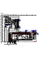
Страница 23: ...23 23 CFD G35 5 6 Schematic Diagram CD Section See page 34 35 for IC Block Diagrams See page 17 for Waveforms ...
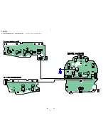
Страница 30: ...30 30 CFD G35 5 14 Printed Wiring Board CONTROL Section See page 17 for Circuit Boards Location SLEEP POWER 25 ...
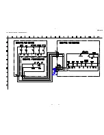
Страница 31: ...31 31 CFD G35 5 15 Schematic Diagram CONTROL Section ...
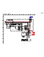
Страница 32: ...32 32 CFD G35 5 16 Printed Wiring Board POWER Section See page 17 for Circuit Boards Location 25 ...
Страница 53: ...53 CFD G35 MEMO ...


