background image

22

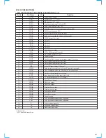
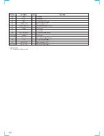
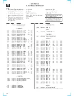
• Abbreviation

EFM : Eight to Fourteen Modulation
PLL : Phase Locked Loop

Pin No.

Pin Name

I/O

Function

TE

CE

RFDC

ADIO

AVSS0

IGEN

AVDD0

ASYO

ASYI

RFAC

AVSS1

CLTV

FILO

FILI

PCO

AVDD1

BIAS

VCTL

V16M

VPCO

DVDD2

ASYE

MD2

DOUT

LRCK

PCMD

BCLK

EMPH

XTSL

DVSS2

XTAI

XTAO

SOUT

SOCK

XOLT

SQSO

SQCK

SCSY

SBSO

EXCK

41

42

43

44

45

46

47

48

49

50

51

52

53

54

55

56

57

58

59

60

61

62

63

64

65

66

67

68

69

70

71

72

73

74

75

76

77

78

79

80

I

I

I

O

I

O

I

I

I

O

I

O

I

I

I/O

O

I

I

O

O

O

O

O

I

I

O

O

O

O

O

I

I

O

I

Tracking error signal input

Center servo analog input

RF signal input

Test pin (Not used)

Analog ground

Stabilized current input for operational amplifiers

Analog power supply

EFM full swing output

Asymmetry comparate voltage input

EFM signal input

Analog ground

Control voltage input for master VCO1

Filter output for master PLL

Filter input for master PLL

Charge-pump output for master PLL

Analog power supply

Asymmetry circuit constant current input

VCO2 control voltage input for wide band EFM PLL (Connected to VDD)

VCO2 oscillator input/output for wide band EFM PLL (Not used)

Charge-pump output for wide band EFM PLL (Not used)

Digital power supply

Asymmetry circuit ON/OFF input

“L” OFF, “H” : ON (Connected to VDD)

Digital-out ON/OFF control input (Connected to VDD)

Digital-out output pin

D/A interface LR clock output (ƒ = Fs)

D/A interface serial data output

D/A interface bit clock output

Playback disc output in emphasis mode (Not used)

X'tal selection input (Connected to ground)

Digital ground

X'tal oscillator circuit input

X'tal oscillator circuit output (Not used)

Serial data output in servo block (Not used)

Serial data read clock output in servo block (Not used)

Serial data latch output in servo block (Not used)

Sub-Q 80-bit and PCM peak level data output (CD text data output)

Clock input for SQSO read-out

Connected to ground

Sub-P through Sub-W serial output (Not used)

Clock input for SBSO read-out (Connected to ground)

Содержание CDP-XB630

Страница 1: ...0 5 dB Signal to noise ratio More than 102 dB Dynamic range More than 98 dB Harmonic distortion Less than 0 0045 Channel separation More than 100 dB Output Jack Maximum Load type output impedance level LINE OUT Phono 2V Over 50 kΩ jacks at 50 kΩ DIGITAL OUT Optical 18 dBm Wave length OPTICAL output 660 nm connector PHONES Stereo 10 mW 32 Ω phone jack General Power requirements 220 V 230 V AC 50 60...

Страница 2: ...uring repairing Do not touch the soldering iron on the same conductor of the circuit board within 3 times Be careful not to apply force on the conductor when soldering or unsoldering 1 SERVICING NOTE 3 2 GENERAL 6 3 DISASSEMBLY 3 1 Front Panel 7 3 2 Base Unit BU 5BD25 7 4 TEST MODE 8 5 ELECTRICAL BLOCK CHECKING 10 6 DIAGRAMS 6 1 Circuit Boards Location 12 6 2 Schematic Diagram Loading Motor Sectio...

Страница 3: ...man body During repair pay attention to electrostatic breakdown and also use the procedure in the printed matter which is included in the repair parts The flexible board is easily damaged and should be handled with care NOTES ON LASER DIODE EMISSION CHECK The laser beam on this model is concentrated so as to be focused on the disc reflective surface by the objective lens in the optical pick up blo...

Страница 4: ... emphasis L R 400Hz 7kHz 4 1 0dB L R 400Hz 7kHz 4 1 10dB L R 19kHz 20kHz 1 1 0dB L R 19kHz 20kHz 1 1 10dB L R 100Hz 0dB L 1kHz 0dB L 10kHz 0dB L 20kHz 0dB L 100Hz 0dB R 1kHz 0dB R 10kHz 0dB R 20kHz 0dB R 100Hz Squer Wave L R 1kHz Squer Wave L R 1kHz w emphasis 0 37dB L R 5kHz w emphasis 4 53dB L R 16kHz w emphasis 9 04dB L R NOTE The contents of Track No 1 to 41 are the same as those of the curren...

Страница 5: ...displayed are not displayed 0 1 2 3 4 5 6 7 8 9 are not displayed A B C D E F G is not displayed H I J K L M N O P Q R S T U VW X Y Z _ A B C D E F G H I J K L M N O P Q R S T U VW X Y Z I are not displayed i are not displayed C ª P R are not displayed 2 3 µ are not displayed 1 º are not displayed À Á Â Ã Ä Å Æ Ç are not displayed È É Ê Ë Ì Í Î Ï Ñ Ò Ó Ô Õ Ö D are not displayed Ù Ú Û Ü Y Ø ß are n...

Страница 6: ... tray 7 0 button 8 EDIT TIME FADE button 9 CHECK button 0 CLEAR button Front Panel AMS knob PUSH ENTER p stop button P pause button play button OPEN CLOSE button Window display LANGUAGE button MUSIC SCAN button ª AUTO SPACE button º PEAK SEARCH button PHONES jack AMS is the abbreviation for Automatic Music Sensor ª º 0 9 8 7 6 3 2 5 4 1 ...

Страница 7: ...1 Turn the cam to the direction of arrow counter clock wise by tapering driver 2 Take off the disc table 3 Yoke bracket BU 5BD25 In order to remove the front panel block when the power supply does not turn on rotate the cam with tapering driver as the figure shows and the loading part will be moved Then pull out the loading part by your hand to remove the loading panel as the figure shows After th...

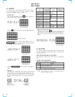
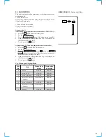
Страница 8: ...essed when the whole display is lit the display will change to partial lighting 2 When the button is pressed the display will light up as follows Partial lighting 5 When the OPEN CLOSE button is pressed all will light up again Key check All buttons have corresponding button numbers When a button is pressed the counter will count up and display the button s num ber However the counter will only cou...

Страница 9: ...hod 2 When no aging mode remote controller 1 Press the U button and turn ON the power 2 Set the disc on the tray 3 Press the OPEN CLOSE button p button and MUSIC SCAN button at the same time If these buttons are not pressed at the same time nothing performs 4 Aging starts and the message shown in Fig 1 is displayed on the fluorescent display tube 5 To end press the U button Fig 1 Message in Aging ...

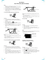
Страница 10: ...more than 10 7 Take sweep time as long as possible and light up the brightness to obtain best waveform oscilloscope BD board TP FE TP VC 1 5 1 symmetry A B Within 3 Vp p 1 5 1 oscilloscope BD board TP FE TP VC symmetry S curve waveform A B Within 3 8 1 1 Vp p S Curve Check Without general remote commander Procedure 1 Connect oscilloscope to test point TP FE on BD board 2 Connect between test point...

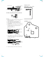
Страница 11: ...he following A B x 100 less than 22 Traverse waveform oscilloscope BD board TP TE TP VC BD BOARD Side A Adjustment Location MAIN BOARD Component Side 0V level 1 3 0 6 Vp p A DC voltage Center of the waveform B 7 Press the 9 button The tracking servo and sledding servo are turned ON Confirm the C DC voltage is almost equal to the A DC voltage is step 6 Traverse waveform 0V C DC voltage Tracking ser...

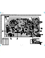
Страница 12: ...12 SECTION 6 DIAGRAMS 6 1 CIRCUIT BOARDS LOCATION DISPLAY board POWER board HEADPHONE board MAIN board BD board LOADING board POWER SW board ...

Страница 13: ...ers refer to waveforms Signal path J CD c digital out For printed wiring boards Note X parts extracted from the component side Y parts extracted from the conductor side p parts mounted on the conductor side Through hole b Pattern from the side which enables seeing The other layers patterns are not indicated Waveforms Caution Pattern face side Parts on the pattern face side seen from the Side B pat...

Страница 14: ...CDP XB630 14 14 6 4 PRINTED WIRING BOARD BD SECTION See page 12 for Circuit Board Location Page 16 A F NP 16 16 ...

Страница 15: ...CDP XB630 15 15 6 5 SCHEMATIC DIAGRAM BD SECTION See page 13 for Waveforms See page 21 for IC Pin Functions See page 25 for IC Block Diagrams Page 17 16 A F NP 5 4 3 2 1 ...

Страница 16: ... 13 14 Ref No Location D401 J 12 D402 J 12 D615 F 10 D616 D 9 D621 G 12 D622 G 13 D631 G 4 D681 G 10 D682 G 10 D691 G 9 D692 G 9 IC601 D 9 IC602 F 8 IC631 G 3 Semiconductor Location Ref No Location IC651 F 14 IC661 D 4 IC671 B 11 IC672 C 11 IC681 D 13 IC801 D 9 IC901 B 4 Q621 G 13 Q681 G 10 Q682 D 13 Q683 F 12 Q691 G 10 Q692 B 13 Q693 G 12 ...

Страница 17: ...CDP XB630 17 17 6 7 SCHEMATIC DIAGRAM MAIN SECTION See page 27 for IC Block Diagrams 13 19 7 8 6 D Page 20 UNREG UNREG UNREG GND 15 ...

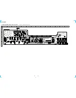
Страница 18: ...CDP XB630 18 18 6 8 PRINTED WIRING BOARD DISPLAY SECTION See page 12 for Circuit Board Location 1 2 A B C D 3 4 5 6 7 8 9 10 11 12 13 14 ...

Страница 19: ...CDP XB630 19 19 6 9 SCHEMATIC DIAGRAM DISPLAY SECTION See page 23 for IC Pin Functions 9 ...

Страница 20: ...ard Location D Page 17 1 2 A B C D E F G H 3 4 5 6 The components identified by mark or dotted line with mark are critical for safety Replace only with part number specified Ref No Location D601 C 4 D602 C 4 D603 C 4 D604 C 4 D605 C 3 D612 C 5 D613 C 5 D614 B 4 D641 B 3 D642 C 3 D643 C 2 Q641 B 3 Semiconductor Location ...

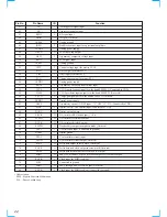
Страница 21: ...t used Sub code sync output 4 2336 MHz output Not used Word clock output ƒ 2Fs Digital ground Numbers of track counted signal input output Not used Mirror signal input output Not used Defect signal input output Not used Focus OK input output Not used Spindle motor external control input Connected to ground GFS is sampled by 460 Hz H when GFS is H Not used Output to control spindle motor servo Inpu...

Страница 22: ...arge pump output for master PLL Analog power supply Asymmetry circuit constant current input VCO2 control voltage input for wide band EFM PLL Connected to VDD VCO2 oscillator input output for wide band EFM PLL Not used Charge pump output for wide band EFM PLL Not used Digital power supply Asymmetry circuit ON OFF input L OFF H ON Connected to VDD Digital out ON OFF control input Connected to VDD D...

Страница 23: ...ion output 20 BUSIN I CONTROL A1 receive input 21 SENSOR SW Not used Open 22 CLK O Serial clock output 23 LDON O Optical pick up laser diode control output 24 DATA O Serial data output 25 SQCK O Subcode Q data readout clock output 26 SUBQ I Subcode Q data input 27 VDD 5V Power supply 5V 28 AVREF I Analog reference voltage input 29 KEY 0 I Key input 30 KEY 1 I Key input 31 KEY 2 I Key input 32 FILT...

Страница 24: ...nected to ground 44 VDD 5V Power supply 5V 45 VFDP 30V Pull down voltage 30V 46 XSEL O Not used 47 Not used 48 LP CONTROL O LP control hold output 49 to 66 OPEN Not used 67 to 87 S21 to S1 O FL segment signal output 88 1G O FL grid signal output 89 VDD 5V Power supply 5V 90 to 100 2G to 12G O FL grid signal output ...

Страница 25: ...Digital CLV MIRR DFCT FOK SERVO Interface CPU Interface OPAmp Analog SW A D Converter PWM GENERATOR FOCUS SERVO SERVO DSP SLED SERVO TRACKING SERVO TRACKING PWM GENERATOR SLED PWM GENERATOR FORCUS PWM GENERATOR 45 SIGNAL PROCESSOR BLOCK SERVO BLOCK MUTE XRST DVDD0 DATA XLAT CLOCK SENS SCLK ATSK WFCK XUGF XPCK GFS SCOR WDCK C4M DVSS0 COUT MIRR V2PO DFCT FOK PWMI LOCK MDP SSTP FETO DVDD1 SFDR SRDR T...

Страница 26: ...CH3 F IN 19 CH3 R IN 18 CAPA IN 3 17 CH3 OUT R 16 CH3 OUT F 15 MUTE LEVEL SHIFT INTERFACE BUFF BUFF BUFF BUFF R F R F BUFF INTERFACE INTERFACE F F R R MUTE 11 12 10 VC VC VC VC VC VC VC VCC VCC RF SUMMING AMP RF_EQ_AMP ERROR AMP FOCUS TRACKING ERROR AMP VC BUFFER VCC VCC VC VC VC VC VEE VEE VEE VEE VEE VREF 13 14 15 6 5 1 2 3 4 7 8 9 16 19 20 21 22 23 24 18 17 HOLD LD PD A B C D VEE F E VC AGCVTH ...

Страница 27: ...2 NOISE FILTER MOTOR DRIVE MOTOR DRIVE MOTOR DRIVE T S D O C P FWD REV STOP CONTROL LOGIC 1 INIT 2 3 4 5 6 7 8 9 10 11 12 13 14 D Vdd 2 SYSM L1 ATT A Vdd L SHIFT L2 LATCH A Vss L 256FSO X Vss TEST1 512IN D Vss X OUT MCKSEL X Vdd XBCK A Vss R DATA R2 LRCK A Vdd R MUTE L R1 MUTE R D Vdd 1 28 27 26 25 24 23 22 21 20 19 18 17 16 15 MODE S P ATT IIR FIR3 FIR2 FIR1 PLM PLM MUTE CIRCUIT CLOCK GENERATOR A...

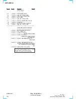
Страница 28: ...ed views are not supplied Hardware mark list and accessories and packing materials are given in the last of this parts list The components identified by mark or dotted line with mark are critical for safety Replace only with part number specified 28 7 1 FRONT PANEL AND CASE SECTION 24 22 23 30 UK model CDM14FL 5BD25 not supplied not supplied not supplied not supplied not supplied Supplied with J40...

Страница 29: ...18 4 997 138 02 CASE 4095269 19 A 4724 737 A POWER BOARD COMPLETE 20 1 433 882 11 TRANSFORMER POWER 21 7 685 885 09 SCREW BVTT 4 16 S 22 1 773 179 11 WIRE FLAT TYPE 23 CORE 23 1 500 386 11 FILTER CLAMP FERRITE CORE 24 4 966 267 11 BUSHING FBS001 CORD 25 1 575 651 21 CORD POWER 26 4 219 386 02 PANEL BACK 27 3 704 515 21 SCREW BV RING 28 1 773 211 11 WIRE FLAT TYPE 25 CORE 29 4 210 291 01 SCREW CASE...

Страница 30: ...110 41 HOLDER MG 103 4 995 814 21 TABLE FL DISC 104 4 967 268 01 GEAR C 105 4 927 649 01 BELT 106 4 933 107 01 GEAR PL 107 4 927 651 01 PULLEY S 108 4 933 109 01 CAM 109 1 645 721 11 LOADING BOARD 110 4 933 134 01 SCREW PTPWH M2 6 6 111 4 959 996 01 SPRING 932 COMPRESSION 112 4 933 129 01 HOLDER BU 113 4 933 111 41 CHASSIS MD 114 4 917 583 21 BRACKET YOKE 115 4 993 142 21 PULLEY L PRESS 116 7 621 ...

Страница 31: ...1 769 069 11 WIRE FLAT TYPE 16 CORE 153 4 917 567 01 GEAR M 154 4 951 940 01 INSULATOR BU 155 4 917 565 01 SHAFT SLED 156 4 917 564 01 GEAR P FLATNESS 157 A 4724 002 A BD BOARD COMPLETE 158 3 713 786 51 SCREW P 2 3 M101 X 4917 523 4 MOTOR ASSY SPINDLE M102 X 4917 504 1 MOTOR ASSY SLED The components identified by mark or dotted line with mark are critical for safety Replace only with part number s...

Страница 32: ...PF 0 25PF 50V C126 1 135 216 11 TANTALUM CHIP 10uF 20 10V C140 1 163 038 91 CERAMIC CHIP 0 1uF 25V C141 1 163 038 91 CERAMIC CHIP 0 1uF 25V C151 1 163 237 11 CERAMIC CHIP 27PF 5 50V C153 1 163 038 91 CERAMIC CHIP 0 1uF 25V C154 1 164 336 11 CERAMIC CHIP 0 33uF 25V C156 1 163 237 11 CERAMIC CHIP 27PF 5 50V C157 1 163 145 00 CERAMIC CHIP 0 0015uF 5 50V C159 1 163 019 00 CERAMIC CHIP 0 0068uF 10 50V ...

Страница 33: ... 1 249 441 11 CARBON 100K 5 1 4W R534 1 249 417 11 CARBON 1K 5 1 4W F R535 1 249 429 11 CARBON 10K 5 1 4W R536 1 249 429 11 CARBON 10K 5 1 4W R537 1 249 429 11 CARBON 10K 5 1 4W R538 1 249 429 11 CARBON 10K 5 1 4W R539 1 249 429 11 CARBON 10K 5 1 4W R541 1 247 807 31 CARBON 100 5 1 4W R542 1 247 807 31 CARBON 100 5 1 4W SWITCH S501 1 762 752 11 SWITCH TACTILE LANC SCAN S502 1 762 752 11 SWITCH TAC...

Страница 34: ...100V C811 1 162 282 31 CERAMIC 100PF 10 50V C901 1 162 282 31 CERAMIC 100PF 10 50V C902 1 161 494 00 CERAMIC 0 022uF 25V C903 1 119 778 31 ELECT 100uF 20 10V C904 1 162 215 31 CERAMIC 47PF 5 50V C905 1 162 215 31 CERAMIC 47PF 5 50V C906 1 130 479 00 MYLAR 0 0047uF 5 50V C907 1 130 473 00 MYLAR 0 0015uF 5 50V C908 1 128 200 51 ELECT 47uF 20 63V C910 1 136 802 11 FILM 0 015uF 5 100V C911 1 162 282 3...

Страница 35: ...06 1 215 461 00 METAL 47K 1 1 4W R907 1 249 419 11 CARBON 1 5K 5 1 4W F R908 1 249 419 11 CARBON 1 5K 5 1 4W F R909 1 249 441 11 CARBON 100K 5 1 4W R910 1 249 414 11 CARBON 560 5 1 4W F R912 1 247 807 31 CARBON 100 5 1 4W R921 1 249 403 11 CARBON 68 5 1 4W F VIBRATOR X671 1 579 834 11 VIBRATOR CRYSTAL 33MHz A 4724 737 A POWER BOARD COMPLETE CAPACITOR C601 1 126 017 11 ELECT 6800uF 20 16V C602 1 12...

Страница 36: ...1 MAGNET ASSY 151 8 848 379 31 OPTICAL PICK UP KSS 213BA F NP 152 1 769 069 11 WIRE FLAT TYPE 16 CORE ACCESSORIES PACKING MATERIALS 1 473 720 11 REMOTE COMMANDER RM DX50 1 551 734 11 CORD CONNECTION 3 866 364 11 MANUAL INSTRUCTION ENGLISH FRENCH SPANISH 3 866 364 21 MANUAL INSTRUCTION GERMAN DUTCH SWEDISH ITALIAN PORTUGUESE AEP 3 866 670 11 MANUAL COMMONNESS INSTRUCTION ENGLISH UK 3 866 670 21 MAN...

Отзывы: