14
CDP-S3
6-2.
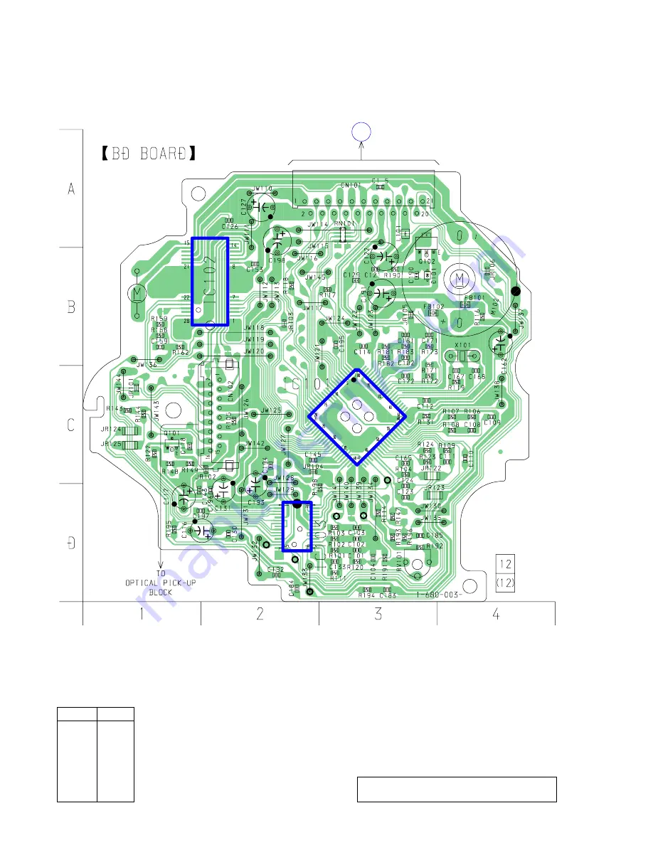
PRINTED WIRING BOARD – BD Section –
•
See page 13 for Circuit Boards Location.
There are a few cases that the part printed on
this diagram isn’t mounted in this model.
• Semiconductor
Location
Ref. No.
Location
MAIN
BOARD
CN301
M102
(SLED)
TP
(RFDC)
TP
(RFAC)
TP
(FEI)
TP
(DVC)
TP (TEO)
TP
(FEO)
M101
(SPINDLE)
A
D101
B-3
IC101
C-3
IC102
B-2
IC103
D-2
Q101
C-1
Q102
A-3
(Page 18)
Содержание CDP-S3
Страница 35: ...35 CDP S3 MEMO ...


