background image

29

6-10.

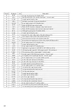
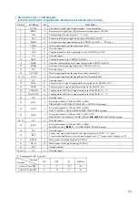
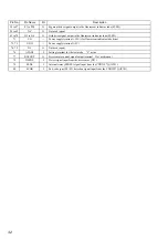
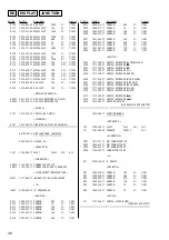
IC  PIN  FUNCTION  DESCRIPTION

• BD BOARD  IC101  CXD2587Q

(DIGITAL SIGNAL PROCESSOR, DIGITAL SERVO PROCESSOR, DIGITAL FILTER, D/A CONVERTER)

Pin No.

Pin Name

I/O

Description

1

SQSO

O

Subcode Q data output to the system controller (IC301)

2

SQCK

I

Subcode Q data reading clock signal input from the system controller (IC301)

3

XRST

I

System reset signal input from the system controller (IC301)    “L”: reset

4

SYSM

I

Analog line muting on/off control signal input terminal    “H”: line muting on 
Not used (fixed at  “L”)

5

DATA

I

Command serial data input from the system controller (IC301)

6

XLAT

I

Command latch pulse input from the system controller (IC301)

7

CLOK

I

Command serial data transfer clock signal input from the system controller (IC301)

8

SENS

O

Internal status monitor output to the system controller (IC301)

9

SCLK

I

SENSE serial data reading clock input from the system controller (IC301)

10

VDD

Power supply terminal (+5V) (digital system)

11

ATSK

I/O

Input pin for anti-shock    Not used (fixed at  “L”)

12

SPOA

I

Microcomputer escape interface input A terminal    Not used (fixed at  “L”) 

13

SPOB

I

Microcomputer escape interface input B terminal    Not used (fixed at  “L”) 

14

XLON

O

Microcomputer escape interface output to the CXA2568M (IC103)

15

WFCK

O

WFCK output terminal     Not used (open)

16

XUGF

O

Not used (open)

17

XPCK

O

Not used (open)

18

GFS

O

Not used (open)

19

C2PO

O

Not used (open)

20

SCOR

O

Subcode sync (S0+S1) detection signal output to the system controller (IC301)

21

COUT

I/O

Numbers of track counted signal input/output terminal    Not used (open)

22

MIRR

I/O

Mirror signal input/output terminal    Not used (open)

23

DFCT

I/O

Defect signal input/output terminal    Not used (open)

24

FOK

I/O

Focus OK input/output terminal    Not used (open)

25

LOCK

I/O

GFS is sampled by 460 Hz    “H” when GFS is “H”    Not used (open)

26

MDP

O

Spindle motor (M101) servo drive signal output to the BA5974FP (IC102)

27

SSTP

I

Limit in detect switch (S101) input terminal

28

SFDR

O

Sled servo drive PWM signal (+) output to the BA5974FP (IC102)

29

SRDR

O

Sled servo drive PWM signal (–) output to the BA5974FP (IC102)

30

TFDR

O

Tracking servo drive PWM signal (+) output to the BA5974FP (IC102)

31

TRDR

O

Tracking servo drive PWM signal (–) output to the BA5974FP (IC102)

32

FFDR

O

Focus servo drive PWM signal (+) output to the BA5974FP (IC102)

33

FRDR

O

Focus servo drive PWM signal (–) output to the BA5974FP (IC102)

34

VSS

Ground terminal (digital system)

35

TEST

I

Input terminal for the test (fixed at “L”)

36

TES1

I

Input terminal for the test (fixed at “L”)

37

XTSL

I

Input terminal for the system clock frequency setting    “L”: 45.1584 MHz, “H”: 22.5792 MHz 
(fixed at “L” in this set)

38

VC

I

Middle point  voltage (+2.5V) input from the CXA2568M (IC103)

39

FE

I

Focus error signal input from the CXA2568M (IC103)

40

SE

I

Sled error signal input from the CXA2568M (IC103)

41

TE

I

Tracking error signal input from the CXA2568M (IC103)

42

CE

I

Command chip enable signal input from the CXA2568M (IC103)

Содержание CDP-CE245 - Compact Disc Player

Страница 1: ...45 CE345 AEP Model UK Model E Model CDP CE345 Australian Model CDP CE245 CE345 SPECIFICATIONS CDP CE245 CE345 Photo CDP CE345 Silver TYPE Model Name Using Similar Mechanism NEW CD Mechanism Type CDM59 5BD32A Base Unit Name BU 5BD32A Optical Pick up Name KSS 213BA F NP ...

Страница 2: ...PARTS WHOSE PART NUMBERS APPEAR AS SHOWN IN THIS MANUAL OR IN SUPPLEMENTS PUB LISHED BY SONY SAFETY CHECK OUT After correcting the original service problem perform the follow ing safety check before releasing the set to the customer Check the antenna terminals metal trim metallized knobs screws and all other exposed metal parts for AC leakage Check leakage as described below LEAKAGE TEST The AC le...

Страница 3: ...air pay attention to electrostatic break down and also use the procedure in the printed matter which is included in the repair parts The flexible board is easily damaged and should be handled with care NOTES ON LASER DIODE EMISSION CHECK The laser beam on this model is concentrated so as to be focused on the disc reflective surface by the objective lens in the optical pick up block Therefore when ...

Страница 4: ...n 6 H button 7 X button 8 x button 9 A OPEN CLOSE button 0 DISC SKIP button qa l AMS L control qs EX CHANGE button qd CLEAR button qf CHECK button qg M button qh m button qj Disc table qk TIME button ql REPEAT button w PROGRAM button wa SHUFFLE button ws CONTINUE button wd PEAK SEARCH button wf EDIT TIME FADE button 1 Voltage selector switch E and Saudi Arabia models only 2 DIGITAL OUT OPTICAL con...

Страница 5: ...ly procedure in the numerical order given SECTION 3 DISASSEMBLY 1 two screws case3 TP2 3 cover 409537 2 two screws BVTP3 8 1 two screws case3 TP2 2 two connectors CN601 602 4 claw 3 three screws BVTP3 8 5 front panel section 4 claw 1 wire flat type 37 core CN301 ...

Страница 6: ...the screw that fixes the table ass y can be seen through around hole in the table ass y 1 Insert a tapering driver from the bottom of the chassis and turn it in the direction of the arrow until the base unit goes down to the lowest position 6 9 CD mechanism deck CDM59 5BD32A a a 3 two screws PTTWH3 6 2 two screws BVTP3 8 5 MAIN board 1 two screws BVTP3 8 4 two PC board holders ...

Страница 7: ...aft into the groove of gear U D gear U D b b TABLE ASS Y Note When installing the table ass y on the chassis ass y engage the gear loading C with the groove by looking into the gear through a hole in the table ass y qs table ass y 9 three screws BTTP M2 6 q clamp e c c d d e qa bracket guide gear loading C 7 two screws BTTP M2 6 5 screw BTTP M2 6 6 bracket guide 2 two screws BTTP M2 6 1 Slide the ...

Страница 8: ...ENSOR BOARD 1 screw PTPWH M2 6 3 belt rotary 4 two screws BTTP M2 6 4 two screws BTTP M2 6 5 SENSOR board 2 tray BELT LOADING LOADING MOTOR BOARD 3 two screws BTTP M2 6 4 LOADING MOTOR board 1 belt loading 2 connector CN13 ...

Страница 9: ...ssis and engage its dowel with the groove of rotary encoder 2 Install the rotary encoder so that its groove comes to the position shown in the figure 1 Insert the shaft gear up to the position where its shaft comes out by 5 mm g g h h f f f 7 gear U D 8 screw PTPWH M2 6 q screw PTPWH M2 6 circle mark circle mark swing gear gear RV Fig A gear U D 9 gear RV Note Align swing gear a circle mark on the...

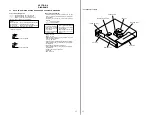
Страница 10: ... and RF SHUFFLE Servo average display 2 TE and Traverse FADER RFCK GFS Error rate display FLUORESCENT INDICATOR TUBE LED ALL LIT AND KEY CHECK MODE 1 Short circuit the test TP2 AFADJ of the MAIN board and ground with a lead wire 2 Press the POWER button to turn ON the power The whole fluorescent indicator tube lights up 3 All buttons have individual button numbers When a button is pressed the butt...

Страница 11: ...alendar numerals light up in ascending order When rotated counterclockwise The music calendar numerals light up in descending order FADER 36 MUSIC SCAN 37 CLEAR 27 CHECK 28 M 29 m 30 PEAK SEARCH 21 TIME 8 TIME TEXT 22 R Light altemately r 1 SEC STEP MIN PEAK TRACK DISC 2 3 4 5 6 7 8 9 10 11 12 13 14 15 16 17 18 19 20 ALL1DISCS PROGRAM SHUFFLE REPEAT 1 EDIT TIME FADE A B All lit SEC MIN TRACK Parti...

Страница 12: ...te controller 1 Press the POWER button and turn ON the power 2 Set discs on all trays More than two discs if five are not available 3 All mode Press the CONTINUE x and CHECK buttons at the same time Disc table mode Press the CONTINUE x and DISC SKIP buttons at the same time Loading mode Press the CONTINUE x and EX CHANGE buttons at the same time 4 Aging starts and the fluorescent indicator tube wi...

Страница 13: ...T buttons simultaneously Loading mode Press the POWER switch while pressing CHECK OPEN CLOSE and TIME buttons simultaneously A A Display contents Mode Check command Display Disc table mode 0 Right one turn r 12 5 Table turning 1 Left one Turn L 10 2 time measurement 2 Measurement end r 12 5 3 Undefined 4 Star position Sta 5 Open Close CLo 10 2 6 Close BU up UP 0 7 Table mode 7 BU up EX open EoP 6 ...

Страница 14: ...pe to TP RF and TP VC on BD board 2 Connect between TP AGCCON and TP GND with lead wire 3 Turned power switch POWER button on 4 Load a disc YEDS 18 and playback 5 Confirm that the oscilloscope waveform is clear and check RF signal level is correct or not 6 After check remove the lead wire connected in step 2 Note Clear RF signal waveform means that the shape can be clearly distinguished at the cen...

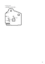
Страница 15: ...15 TP VC TP RF TP FE TP TE TP FE1 TP GND TP PLCK TP AGCCON CN102 IC101 Checking Location BD BOARD Conductor Side ...

Страница 16: ...16 MEMO ...
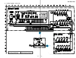
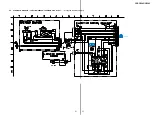
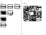
Страница 17: ...impedance 10 MΩ Voltage variations may be noted due to normal produc tion tolerances Waveforms are taken with a oscilloscope Voltage variations may be noted due to normal produc tion tolerances Circled numbers refer to waveforms Signal path J CD PLAY Note The components identi fied by mark 0 or dotted line with mark 0 are criti cal for safety Replace only with part number specified Note Les compos...

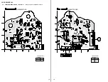
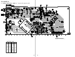
Страница 18: ...7 for Circuit Boards Location A 05 05 TP GND TP FE1 TP RF TP VC TP FE TP TE TP AGCCON TP PLCK LIMIT SPINDLE SLED CONDUCTOR SIDE COMPONENT SIDE Page 22 Semiconductor Location Ref No Location Q101 C 3 Semiconductor Location Ref No Location IC101 C 2 IC102 B 1 IC103 B 1 ...

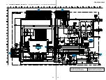
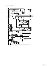
Страница 19: ...Block Diagrams PIN FUNCTION Page 23 The components identified by mark 0 or dotted line with mark 0 are critical for safety Replace only with part number specified Les composants identifiés par une marque 0 sont critiques pour la sécurité Ne les remplacer que par une pièce portant le numéro spécifié ...

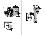
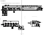
Страница 20: ...20 CDP CE245 CE345 6 4 PRINTED WIRING BOARDS JUNCTION SENSOR LOADING MOTOR Boards See page 17 for Circuit Boards Location TO LOADING MOTOR BOARD TO JUNCTION BOARD Page 22 TO SENSOR BOARD TO JUNCTION BOARD ...

Страница 21: ...21 21 CDP CE245 CE345 6 5 SCHEMATIC DIAGRAM JUNCTION SENSOR LOADING MOTOR Boards See page 26 for IC Block Diagram Page 23 ...

Страница 22: ...02 D 7 IC603 E 7 Q301 C 10 Q307 B 8 Q352 A 5 Q353 A 4 Q356 C 2 Q402 B 1 Q405 B 1 Q502 A 1 Q505 A 1 Q601 E 7 Ref No Location Ref No Location D350 A 5 D351 A 5 D353 C 3 D601 C 6 D602 D 6 D603 D 6 D604 D 6 D605 E 6 D606 E 6 D607 C 5 D608 C 5 D609 C 5 IC301 C 9 IC303 B 1 Semiconductor Location Page 24 Page 18 Page 20 Page 24 ...

Страница 23: ...ams PIN FUNCTION Page 25 Page 19 Page 25 Page 21 The components identified by mark 0 or dotted line with mark 0 are critical for safety Replace only with part number specified Les composants identifiés par une marque 0 sont critiques pour la sécurité Ne les remplacer que par une pièce portant le numéro spécifié ...

Страница 24: ...24 24 CDP CE245 CE345 6 8 PRINTED WIRING BOARDS PANEL Section See page 17 for Circuit Boards Location Page 22 TO DISPLAY BOARD TO KEY BOARD Page 22 ...

Страница 25: ...ge 23 The components identified by mark 0 or dotted line with mark 0 are critical for safety Replace only with part number specified Les composants identifiés par une marque 0 sont critiques pour la sécurité Ne les remplacer que par une pièce portant le numéro spécifié ...

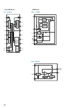
Страница 26: ...UT1 BCK LRCK PCMD LMUT AVSS1 AVSS2 CPU INTERFACE SERVO AUTO SEQUENCER SERIAL IN INTERFACE OVER SAMPLING DIGITAL FILTER 3rd ORDER NOISE SHAPER PWM PWM EFM DEMODULATOR TIMING LOGIC DIGITAL OUT D A INTERFACE DIGITAL PLL ASYMMETRY CORRECTION CLOCK GENERATOR MIRR DFCT FOK DETECTOR DIGITAL CLV SUBCODE PROCESSOR SERVO INTERFACE SERVO DSP FOCUS SERVO TRACKING SERVO SLED SERVO PWM GENERATOR FOCUS PWM GENER...

Страница 27: ...RROR AMP TRACKING ERROR AMP VC BUFFER VCC 50µA VEE VEE VC VC VC VC VC VC VC VC VC VC VCC VEE VCC VEE VEE VC VCC LC PD LD ON HOLD SW AGC CONT RFTC RF I RF O RFE TE FE RF BOT HOLD AGC VTH LD PD A B C D VEE F E VC 1 2 3 4 5 6 7 8 9 10 11 12 13 14 15 16 17 18 19 20 21 22 23 24 VCC ...

Страница 28: ... DETECTION AMPLIFIER COVERNER OUTPUT REFERENCE VOLTAGE OUTPUT LOW VOLTAGE OUTPUT RIN1 IOUT VEE VEE VCC VREF VREG VCC OUT1 OUT1 18 17 16 15 1 2 3 4 5 6 7 8 9 14 13 12 11 10 1 2 3 4 5 7 6 V IN EN GND CDEL CN RES V OUT REFERENCE VOLTAGE OVER HEAT PROTECTION OVER CURRENT LIMITTER ON OFF RESET GEN ERROR AMP 2 5 5k 27k OVERCURRENT LIMITTER OVERHEAT PROTECTION REFERENCE VOLTAGE GND ON OFF IN REFERENCE VO...

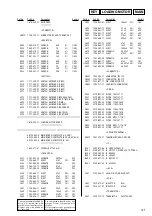
Страница 29: ...PO O Not used open 20 SCOR O Subcode sync S0 S1 detection signal output to the system controller IC301 21 COUT I O Numbers of track counted signal input output terminal Not used open 22 MIRR I O Mirror signal input output terminal Not used open 23 DFCT I O Defect signal input output terminal Not used open 24 FOK I O Focus OK input output terminal Not used open 25 LOCK I O GFS is sampled by 460 Hz ...

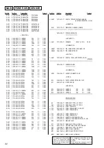
Страница 30: ... supply terminal 5V digital system 60 DOUT O Digital audio signal output to the DIGITAL OUT OPTICAL IC303 61 LRCK O L R sampling clock signal 44 1 kHz output terminal Not used open 62 PCMD O D A interface serial data output terminal Not used open 63 BCK O Bit clock signal 2 8224 MHz output terminal Not used open 64 EMPH O De emphasis control signal output terminal Not used open 65 XVDD Power suppl...

Страница 31: ...etect switch S11 15 16 S1 S2 I Detect signal input from the tray address detect switch S200 17 NC O Not used open 18 TBLL O Table motor drive signal counterclockwise output to the BA6780 IC11 19 TBLR O Table motor drive signal clockwise output to the BA6780 IC11 20 LOAD IN O Loading motor M11 drive signal output to the BA6780 IC11 1 21 LOAD OUT O Loading motor M11 drive signal output to the BA6780...

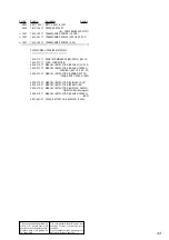
Страница 32: ...wer supply terminal 30V for fluorescent indicator tube drive 72 73 VDD Power supply terminal 5V 74 75 NC O Not used open 76 AFADJ I Setting terminal for the test mode L active 77 BUSOUT O Sircs remote control signal output terminal Not used open 78 DSENS I Detect signal input from the disc sensor D11 79 SENS I Internal status SENSE signal input from the CXD2587Q IC101 80 SCOR I Sub code sync S0 S1...

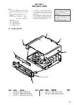
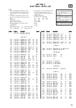
Страница 33: ...plied Accessories and packing materials are given in the last of the electrical parts list NOTE XX and X mean standardized parts so they may have some difference from the original one Color Indication of Appearance Parts Example KNOB BALANCE WHITE RED Parts Color Cabinet s Color Abbreviation AUS Australian model CND Canadian model EA Saudi Arabia model SP Singapore model Ref No Part No Description...

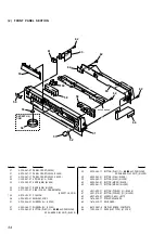
Страница 34: ... 57 4 224 866 11 WINDOW FL CE345 58 4 224 864 01 BUTTON PLAY H X x A OPEN CLOSE EX CHANGE DISC SKIP BLACK 58 4 224 864 11 BUTTON PLAY H X x A OPEN CLOSE EX CHANGE DISC SKIP SILVER 59 4 224 862 01 BUTTON DISC BLACK 59 4 224 862 11 BUTTON DISC SILVER 60 4 224 863 01 BUTTON MODE BLACK 60 4 224 863 11 BUTTON MODE SILVER 61 3 931 429 21 BUTTON POWER BLACK 61 4 227 979 01 BUTTON POWER SILVER 62 4 951 62...

Страница 35: ...2 N S 109 4 224 877 01 PANEL BACK CE245 US 109 4 224 877 11 PANEL BACK CE245 CND 109 4 224 877 41 PANEL BACK CE245 AUS 109 4 224 878 01 PANEL BACK CE345 US 109 4 224 878 11 PANEL BACK CE345 CND 109 4 224 878 21 PANEL BACK CE345 AEP 109 4 224 878 31 PANEL BACK CE345 UK 109 4 224 878 41 PANEL BACK CE345 AUS 109 4 224 878 52 PANEL BACK CE345 E 109 4 224 878 61 PANEL BACK CE345 SP 109 4 224 878 71 PAN...

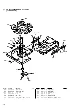
Страница 36: ... 1 ROLLER ASSY 204 4 224 602 01 TABLE 205 4 224 617 01 GEAR RM E 206 4 985 672 01 SCREW PTPWH M2 6 FLOATING 207 4 224 616 01 GEAR RM M 208 4 224 615 01 GEAR RM B 209 4 225 328 01 BELT ROTARY 210 4 224 603 01 TRAY 211 4 224 619 01 BRACKET GUIDE M11 A 4672 867 A MOTOR ASSY ROTARY TRAY 201 202 202 203 203 205 206 207 208 203 206 209 202 not supplied 204 M11 210 206 211 202 202 211 not supplied ...

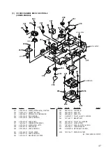
Страница 37: ...NG C 261 4 224 608 01 COLLAR SWING 262 4 224 611 01 GEAR LOADING B 263 3 016 533 21 WASHER FR STOPPER 264 4 951 619 21 CUSHION A 265 4 224 606 01 GEAR RV 266 4 224 605 01 GEAR U D 267 X 4952 019 1 PULLEY A ASSY CHUCKING 268 1 471 061 11 MAGNET ASSY 269 4 221 688 01 PULLEY B CHUCKING 270 4 224 618 01 LEVER LIFTER 271 1 791 930 11 WIRE FLAT TYPE 6 CORE 272 1 676 246 11 JUNCTION BOARD M10 A 4672 879 ...

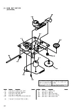
Страница 38: ...ifié Ref No Part No Description Remark Ref No Part No Description Remark 301 4 951 620 01 SCREW 2 6X8 BVTP 302 A 4724 494 A BD BOARD COMPLETE 303 4 951 940 41 INSULATOR BU 304 4 917 565 01 SHAFT SLED 0305 8 848 379 31 OPTICAL PICK UP KSS 213BA F NP 306 1 769 069 11 WIRE FLAT TYPE 16 CORE 307 3 713 786 51 SCREW P 2X3 308 4 917 567 21 GEAR M 309 4 917 564 01 GEAR P FLATNESS M101 X 4917 523 3 MOTOR A...

Страница 39: ...IC CHIP 0 001uF 10 50V C172 1 163 123 00 CERAMIC CHIP 180PF 5 50V C181 1 163 009 11 CERAMIC CHIP 0 001uF 10 50V C182 1 163 123 00 CERAMIC CHIP 180PF 5 50V CONNECTOR CN101 1 784 360 11 CONNECTOR FFC LIF NON ZIF 21P CN102 1 777 937 11 CONNECTOR FFC FPC 16P FERRITE BEAD FB101 1 500 445 21 FERRITE 0uH FB103 1 500 445 21 FERRITE 0uH IC IC101 8 752 386 85 IC CXD2587Q IC102 8 759 549 28 IC BA5974FP E2 IC...

Страница 40: ...17 11 CARBON 1K 5 1 4W R813 1 249 419 11 CARBON 1 5K 5 1 4W R814 1 249 421 11 CARBON 2 2K 5 1 4W R815 1 247 843 11 CARBON 3 3K 5 1 4W R816 1 249 427 11 CARBON 6 8K 5 1 4W R817 1 249 415 11 CARBON 680 5 1 4W R818 1 249 417 11 CARBON 1K 5 1 4W R819 1 249 419 11 CARBON 1 5K 5 1 4W R820 1 249 421 11 CARBON 2 2K 5 1 4W R821 1 247 843 11 CARBON 3 3K 5 1 4W R822 1 249 427 11 CARBON 6 8K 5 1 4W R823 1 249...

Страница 41: ...1 CERAMIC 470PF 10 50V C602 1 126 936 11 ELECT 3300uF 20 16V C603 1 126 942 61 ELECT 1000uF 20 16V C604 1 126 963 11 ELECT 4 7uF 20 50V C605 1 126 963 11 ELECT 4 7uF 20 50V C606 1 126 963 11 ELECT 4 7uF 20 50V C607 1 126 941 11 ELECT 470uF 20 6 3V C608 1 104 666 11 ELECT 220uF 20 10V C609 1 128 552 11 ELECT 47uF 20 63V C610 1 126 964 11 ELECT 10uF 20 50V C611 1 126 767 11 ELECT 1000uF 20 16V C612 ...

Страница 42: ... 1 4W R422 1 249 421 11 CARBON 2 2K 5 1 4W R501 1 215 453 00 METAL 22K 1 1 4W R502 1 215 425 00 METAL 1 5K 1 1 4W R503 1 215 425 00 METAL 1 5K 1 1 4W R504 1 215 445 00 METAL 10K 1 1 4W R505 1 215 443 00 METAL 8 2K 1 1 4W R506 1 215 469 00 METAL 100K 1 1 4W R514 1 215 405 00 METAL 220 1 1 4W R515 1 215 405 00 METAL 220 1 1 4W R519 1 249 421 11 CARBON 2 2K 5 1 4W R520 1 215 405 00 METAL 220 1 1 4W R...

Страница 43: ...226 518 21 MANUAL INSTRUCTION ENGLISH FRENCH SPANISH AEP UK E EA SP 4 226 518 31 MANUAL INSTRUCTION GERMAN DUTCH ITALIAN PORTUGUESE AEP 4 226 518 41 MANUAL INSTRUCTION CHINESE E SP 4 226 518 51 MANUAL INSTRUCTION ARABIC EA 4 226 518 61 MANUAL INSTRUCTION SWEDISH DANISH FINNISH North European 4 226 518 71 MANUAL INSTRUCTION ENGLISH FRENCH CND 4 981 643 01 COVER BATTERY for RM DC355 CE345 The compon...

Страница 44: ...44 CDP CE245 CE345 Sony Corporation Home Audio Division Company 9 929 204 11 2000C0585 1 Printed in Japan C 2000 3 Published by Quality Assurance Dept ...

Отзывы: