background image

– 27 –

5-6.

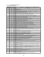
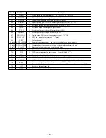
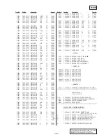
IC  PIN  FUNCTION  DESCRIPTION

 IC801 (SYSTEM CONTROLLER)

 TMP88CM22F-1A28 (EXCEPT US: TYPE A), TMP88CM22F-1A35 (EXCEPT US: TYPE B), TMP88CM22F-1A42 (US) 

Pin No.

Pin Name

I/O

Description

1

VSS

Ground terminal

2

IRRMC

I

Not used (Fixed at “L”)

3

FOKI

I

Focus OK signal input from the digital servo processor (IC601)    “L”: NG, “H”: OK

4

AGCCON

O

AGC control pulse signal output terminal

5

XLEDDISP

O

CHG/HOLD LED control signal output terminal    Not used (open)

6

VCC

SWITCHING

O

Control signal output terminal for the switching power supply circuit

7

AMUTE

O

Analog audio muting ON/OFF control signal output terminal    “H”: muting ON

8

VCC2 ON

O

VCC2 voltage control signal output terminal

9

XRST

O

Reset signal output to the CXD3027R (IC601)    “L”: reset

10

SCK

O

Serial data transfer clock signal output to the CXD3027R (IC601)

11

SDTI

I

Serial data input from the CXD3027R (IC601)

12

SDTO

O

Serial data output to the CXD3027R (IC601)

13

SLPOUT

O

WAKE-UP control signal output terminal (for system standby reset)

14

SEL

I

Plug-in detection signal input terminal of LINE OUT/OPTICAL OUT

15

CHGMNT1

I

Battery charge voltage detection input from the power control (IC401)

16

VCDKEY

I

Key input from the S809, S810 (/–) and switch unit (A/D input)

17

BATMNT

I

Battery voltage detection signal input terminal

18

KEY

I

Key input from the switch unit (A/D input)

19

RMKEY

I

Key input from the headphone with remote commander (A/D input)

20

DCINMNT

I

DC input voltage detection input terminal (A/D input)  and DC input jack use/no use detection
input terminal

21

OPEN

I

CD door open/close detection switch (S801) input terminal
The stop status is reset with the falling edge of input signal

22

VREFL

I

Reference voltage input terminal (0V) for A/D converter

23

VREFH

I

Reference voltage input terminal (+2V) for A/D converter

24

VDD

Power supply terminal (+2V)

25

SCOR

I

Sub-code sync (S0+S1) detection signal input from the CXD3027R (IC601)

26

GRSCOR

I

Communication clock signal input from the CXD3027R (IC601)

27

FG

I

FG pulse signal input from the spindle motor driver (IC402)

28

BEEP

O

Beep sound output to the headphone amplifier (IC351)

29

NC

Not used (Fixed at “H”)

30

RMSCK

O

Communication clock output to the communication format converter (IC802)

31

RMDATI

I

Communication data bus input of headphone with remote commander from the communication
format converter (IC802)

32

RMDATO

O

Communication data bus output of headphone with remote commander to the communication
format converter (IC802)

33

RMRW

O

Read/write control signal output of headphone with remote commander to the communication
format converter (IC802)     “L”: read mode, “H”: write mode

34

RMLAT

O

Serial data latch pulse signal output of headphone with remote commander to the communication
format converter (IC802)

35

WFCKI

I

Demodulation signal input from the CXD3027R (IC601)

36

COMPON I

I

Not used (open) (Only US model: pull up)

37

XNTSC

I

Not used (Fixed at “H”)

38

AVLS

I

AVLS (Automatic Volume Limiter System) switch (S803) input terminal
“L”: normal mode, “H”: limit mode

Содержание CD Walkman D-E880

Страница 1: ...IONS D E880 EJ815 Photo D EJ815 Silver model US Model E Model Chinese Model D EJ815 Tourist Model D E880 Model Name Using Similar Mechanism NEW CD Mechanism Type US CDM 3022EBG Other CDM 3022EBA Optical Pick Up Name US DAX 22G Other DAX 22E Ver 1 0 1999 10 ...

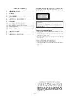
Страница 2: ...RITICAL TO SAFE OPERATION REPLACE THESE COMPONENTS WITH SONY PARTS WHOSE PART NUMBERS APPEAR AS SHOWN IN THIS MANUAL OR IN SUPPLEMENTS PUB LISHED BY SONY TABLE OF CONTENTS 1 SERVICING NOTES 3 2 GENERAL 4 3 DISASSEMBLY 5 4 ELECTRICAL ADJUSTMENTS 7 5 DIAGRAMS 5 1 Block Diagram MAIN Section 1 2 9 5 2 Block Diagram MAIN Section 2 2 11 5 3 Block Diagram POWER SUPPLY Section 13 5 4 Printed Wiring Board ...

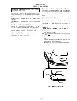
Страница 3: ...in the optical pick up so that the light focuses on the reflection surface of the disc Therefore be sure to keep your eyes more then 30 cm apart from the object lens when you check the emission of laser diode Laser Diode Checking Methods During normal operation of the equipment emission of the laser diode is prohibited unless the upper lid is closed while turning ON the S801 push switch type The f...

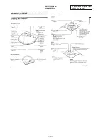
Страница 4: ... 4 SECTION 2 GENERAL This section is extracted from instruction manual ...

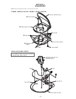
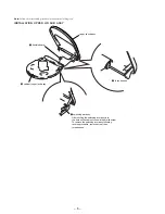
Страница 5: ...he upper lid sub assy 2 three screws B2 5 cabinet upper sub assy 3 three claws 4 flexible board CN801 3 two claws 2 two screw B2 6 cabinet lower sub assy 3 five claws S804 knob HOLD cabinet lower sub assy knob AVLS S803 CDM 3022EBA EXCEPT US CDM 3022EBG US INSTALLATION MAIN BOARD On installation MAIN board adjust the S803 804 and knobs HOLD AVLS ...

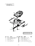
Страница 6: ...rm assy upper lid sub assy 3 three bosses After sticking the switching arm assy into the hole on the cabinet connect them with screw To remove the switching arm assy following reverse procedure remove screw then three bosses Note Follow the disassembly procedure in the numerical order given ...

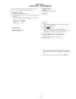
Страница 7: ...Condition Hold the set in horizontal state Connection Procedure 1 Connect the oscilloscope to the test points TP601 RF and TP GND on the MAIN board 2 Set a disc YEDS 18 3 Press the u button 4 Check the oscilloscope waveform is as shown below A good eye pattern means that the diamond shape in the center of the waveform can be clearly distinguished RF Signal reference Waveform Eye Pattern VOLT DIV 1...

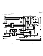
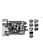
Страница 8: ... TRDR M901 SLED FOCUS TRACKING FI2 RI2 FI1 RI1 FI3 FI3 FO2 RO2 FO1 RO1 FO3 RO3 FOCUS TRACKING COIL DRIVER SLED MOTOR DRIVER IC401 2 2 M 78 83 28 26 30 35 24 25 23 3 26 35 11 44 43 10 12 25 MODE CONTROL ROTATION DETECTOR BEMF SEPARATOR PREDRIVER FEEDBACK PATTERN GENERATOR OR PHASE PWM DECODER 44 MDS 43 MDP 17 SCOR 42 4 1 3 2 23 24 25 14 16 18 20 45 27 41 22 C176 FOK R4M XIN 42 XHGON 39 HOLD 21 OPEN...

Страница 9: ...KEY 4 3 2 1 VCPU 2V OFF ON S803 AVLS VCPU 2V IN_R IN_L HEADPHONE AMP IC351 14 HEADPHONE ON OFF SWITCH IC302 1 7 2 15 OUT_R OUT_L 8 6 PW_SW MT_SW 19 BEEP 17 PW SW BEEP MT SW 20 6 3 5 TAP802 TEST LOUT2 LOUT1 I J L K VOLUME S810 S809 50 64 SEG14 ı SEG0 COM3 ı COM0 65 68 31 RMDATI 32 RMDATO 30 RMSCK 34 RMLAT 33 RMRW 78 MICRO COMPUTER INTERFACE REMOTE CONTROL INTERFACE 18 RW 17 XLT 16 SCK 15 19 SO TSB ...

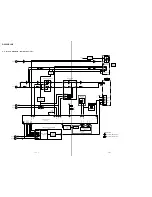
Страница 10: ...TCHING Q414 SWITCHING POWER CIRCUIT 1 LENEAR REGULATOR SYSTEM CONTROL INPUT OUTPUT VG POWER CIRCUIT LOW VOLTAGE DETECTOR CLOCK 57 51 52 43 44 42 45 63 41 CHG SW RF4 INM4 RF21 RF21 RF2 RF2 VC VC VCP VCP INM2 INM2 APCREF APCREF PAPC PA PC MODE2 MODE2 MODE1 MODE1 WAKEUP LATCHC DATA CLOCK DATA CLOCK VLG2O SYNC 14 13 67 8 7 3 12 48 47 15 2 55 59 50 46 49 4 56 11 SDTO SCK PD 13 LD D F G B A H SYNC DTC2D...

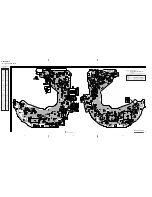
Страница 11: ...E 13 Q408 E 13 Q409 B 15 Q411 G 3 Q412 B 7 Q413 B 15 Q414 C 13 Q416 D 14 Q601 I 15 Q602 H 5 Q603 I 5 Q604 G 3 Q801 I 5 Note on Printed Wiring Board X parts extracted from the component side Y parts extracted from the conductor side a Through hole b Pattern from the side which enables seeing The other layers patterns are not indicated Caution Pattern face side Parts on the pattern face side seen fr...

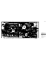
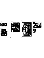
Страница 12: ...tage is dc 4 5V and fed with regulated dc power supply from CDIN jack J401 Voltages and waveforms are dc with respect to ground in playback mode no mark CD PLAY Voltages are taken with aVOM Input impedance 10 MΩ Voltage variations may be noted due to normal produc tion tolerances Waveforms are taken with a oscilloscope Voltage variations may be noted due to normal produc tion tolerances Circled nu...

Страница 13: ...CUS SERVO SLED SERVO TRACKING SERVO CLOCK GENERATOR LPF LPF MIRR DFCT FOK PWM GENERATOR FOCUS PWM GENERATOR SLED PWM GENERATOR TRACKING PWM GENERATOR 90 89 88 87 86 85 84 83 82 81 80 79 78 77 76 75 74 73 72 71 70 69 68 67 66 65 64 63 62 61 1 2 3 4 5 6 7 8 9 10 11 12 13 14 15 16 17 18 19 20 21 22 23 24 25 26 27 28 29 30 31 32 33 34 35 36 37 38 39 40 41 42 43 44 45 46 47 48 49 50 51 52 53 54 55 56 5...

Страница 14: ...er A D input 20 DCINMNT I DC input voltage detection input terminal A D input and DC input jack use no use detection input terminal 21 OPEN I CD door open close detection switch S801 input terminal The stop status is reset with the falling edge of input signal 22 VREFL I Reference voltage input terminal 0V for A D converter 23 VREFH I Reference voltage input terminal 2V for A D converter 24 VDD Po...

Страница 15: ... 50 to 64 SEG14 to SEG0 O Segment drive signal output to the liquid crystal display on the switch unit 65 to 68 COM3 to COM1 O Common drive signal output to the liquid crystal display on the switch unit 69 to 71 V3 to V1 O Bias signal output to the liquid crystal display driver 72 73 C1 C0 O Capacitor connected terminal for the liquid crystal display driver voltage up 74 STOP O VCD control stop si...

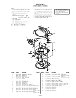
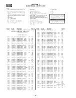
Страница 16: ...33 100 240V AC area in E model HK Hong Kong model 9 10 9 11 12 1 13 14 8 7 5 1 2 3 4 6 7 17 16 15 18 18 1 3 318 382 01 SCREW 1 7X3 TAPPING 2 X 4952 203 1 OPEN ASSY 3 4 224 016 01 KNOB OPEN 4 4 224 786 01 LEVER DETECTION 5 3 375 114 51 SCREW 6 1 674 587 11 SWITCH BOARD 7 4 908 792 91 SCREW B2 8 4 224 015 01 BUTTON VOL 9 3 345 710 21 SCREW M1 4X3 TAPPING 10 X 4952 200 1 LID SUB ASSY UPPER FOR SILVER...

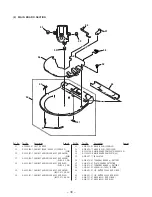
Страница 17: ...CABINET LOWER SUB ASSY FOR SILVER EJ815 E13 HK CH 52 X 4952 331 1 CABINET LOWER SUB ASSY FOR BLUE EJ815 E13 HK CH 53 4 224 020 01 KNOB HOLD FOR BLUE 53 4 224 020 11 KNOB HOLD FOR SILVER 54 A 3323 346 A MAIN BOARD COMPLETE EXCEPT US 54 A 3323 459 A MAIN BOARD COMPLETE US 55 4 221 927 11 INSULATOR 56 4 224 012 01 TERMINAL BOARD BATTERY 57 4 224 014 01 PLATE CHARGE DETECTION 58 4 224 013 01 TERMINAL ...

Страница 18: ...0101 X 3378 495 1 OPTICAL PICK UP DAX 22EG US 0101 X 4952 079 1 OPTICAL PICK UP DAX 22E EXCEPT US 102 3 704 197 92 SCREW M1 4X1 8 LOCKING 103 4 220 645 01 SHAFT STANDARD 104 4 220 646 01 RACK 105 A 3328 298 A SCREW ASSY FEED 106 3 338 645 31 WASHER 0 8 2 5 107 3 686 458 03 SCREW P1 4X3 5 TAPPING 108 4 220 648 01 GEAR C 109 X 4951 688 1 BRACKET ASSY SLED 110 3 348 998 61 SCREW M1 4X4 TAPPING PAN 11...

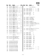
Страница 19: ... C406 1 164 156 11 CERAMIC CHIP 0 1uF 25V C407 1 125 899 11 TANTALUM CHIP 220uF 20 4V C408 1 109 982 11 CERAMIC CHIP 1uF 10 10V C409 1 162 970 11 CERAMIC CHIP 0 01uF 10 25V C410 1 110 569 11 TANTALUM CHIP 47uF 20 4V C412 1 162 970 11 CERAMIC CHIP 0 01uF 10 25V C413 1 162 964 11 CERAMIC CHIP 0 001uF 10 50V C414 1 104 913 11 TANTALUM CHIP 10uF 20 16V C415 1 115 566 11 CERAMIC CHIP 4 7uF 10 10V C416 ...

Страница 20: ...17 13B D404 8 719 049 09 DIODE 1SS367 T3SONY D405 8 719 077 01 DIODE CRS03 TE85L D406 8 719 077 01 DIODE CRS03 TE85L D409 8 719 049 09 DIODE 1SS367 T3SONY D410 8 719 049 09 DIODE 1SS367 T3SONY D411 8 719 049 09 DIODE 1SS367 T3SONY D412 8 719 049 09 DIODE 1SS367 T3SONY D413 8 719 049 09 DIODE 1SS367 T3SONY D414 8 719 049 09 DIODE 1SS367 T3SONY D415 8 719 049 09 DIODE 1SS367 T3SONY D416 8 719 049 09...

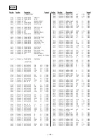
Страница 21: ...0 5 1 16W R404 1 218 888 11 METAL CHIP 51K 0 5 1 16W R405 1 218 887 11 METAL CHIP 47K 0 5 1 16W R406 1 218 889 11 METAL CHIP 56K 0 5 1 16W R407 1 216 839 11 METAL CHIP 33K 5 1 16W R408 1 216 841 11 METAL CHIP 47K 5 1 16W R409 1 216 833 11 RES CHIP 10K 5 1 16W R410 1 216 833 11 RES CHIP 10K 5 1 16W R411 1 216 847 11 METAL CHIP 150K 5 1 16W R412 1 216 839 11 METAL CHIP 33K 5 1 16W R414 1 218 917 11 ...

Страница 22: ...P 22K 5 1 16W R812 1 216 864 11 METAL CHIP 0 5 1 16W R813 1 216 833 11 RES CHIP 10K 5 1 16W R814 1 216 833 11 RES CHIP 10K 5 1 16W R815 1 216 864 11 METAL CHIP 0 5 1 16W R816 1 216 864 11 METAL CHIP 0 5 1 16W US R817 1 216 864 11 METAL CHIP 0 5 1 16W R819 1 216 864 11 METAL CHIP 0 5 1 16W R820 1 216 864 11 METAL CHIP 0 5 1 16W R821 1 216 864 11 METAL CHIP 0 5 1 16W R822 1 216 864 11 METAL CHIP 0 5...

Страница 23: ...6 035 31 BATTERY PACK NC WMAA EJ815 US 3 043 927 11 MANUAL INSTRUCTION ENGLISH EJ815 US 3 867 736 01 MANUAL INSTRUCTION JAPANESE ENGLISH CHINESE KOREA E880 3 867 736 11 MANUAL INSTRUCTION SPANISH E880 EJ815 E33 3 867 736 21 MANUAL INSTRUCTION ENGLISH E880 EJ815 US E33 3 043 840 01 CASE CARRYING US 4 223 953 01 CASE MIS CARRYING EXCEPT US 8 953 276 90 HEADPHONE MDR 24SP SET EJ815 US 8 953 304 90 RE...

Отзывы: