4
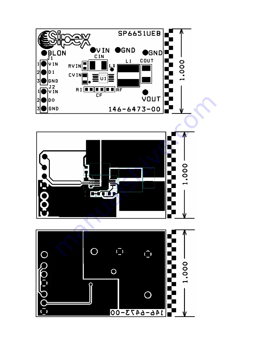
EVALUATION BOARD LAYOUT
FIGURE 3: SP6651AEU COMPONENT PLACEMENT
FIGURE 4: SP6651AEU PC LAYOUT TOP SIDE
FIGURE 5: SP6651AEU PC LAYOUT BOTTOM SIDE
Страница 1: ...verter performance FIGURE 1 SP6651A 3 3V OUTPUT EVALUATION BOARD SCHEMATIC High Efficiency Synchronous Step Down Converter with up to 98 efficiency 800mA Output Current only 20uA Quiescent Current 2 7...
Страница 2: ...e Definition D1 D0 Definition 0 0 Shutdown All internal circuitry is disabled and the power switches are opened 0 1 Device enabled falling UVLO threshold 2 70V 1 0 Device enabled falling UVLO threshol...
Страница 3: ...from FB to ground and FB to Vout to control the output voltage This pin regulates to the internal reference voltage of 0 8V 6 Vout Output voltage sense pin Used for internal timing and BLON circuitry...
Страница 4: ...4 EVALUATION BOARD LAYOUT FIGURE 3 SP6651AEU COMPONENT PLACEMENT FIGURE 4 SP6651AEU PC LAYOUT TOP SIDE FIGURE 5 SP6651AEU PC LAYOUT BOTTOM SIDE...
Страница 5: ...5 ORDERING INFORMATION Model Temperature Range Package Type SP6651EB 40 C to 85 C SP6651 Evaluation Board...