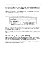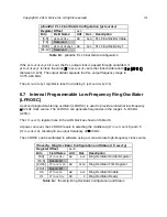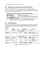
pllcfg: PLL Configuration and Status (
pllcfg
)
Register Offset
0x8
Bits
Field Name
Attr.
Rst.
Description
[2:0]
pllr
RW
0x1
PLL R Value
3
Reserved
[9:4]
pllf
RW
0x1F
PLL F Value
[11:10]
pllq
RW
0x3
PLL Q Value
[15:12]
Reserved
16
pllsel
RW
0x0
PLL Select
17
pllrefsel
RW
0x1
PLL Reference Select
18
pllbypass
RW
0x1
PLL Bypass
[30:19]
Reserved
31
plllock
RO
X
PLL Lock
Figure 3 shows how the PLL output frequency is set using a combination of three read-write
fields:
pllr[2:0]
,
pllf[2:0]
,
pllq[1:0]
. The frequency constraints must be observed
between each stage for correct operation.
Figure 3:
Controlling the FE310-G002 PLL output frequency.
The
pllr[1:0]
field encodes the reference clock divide ratio as a 2-bit binary value, where the
value is one less than the divide ratio (i.e.,
00
=1,
11
=4). The frequency of the output of the refer-
ence divider (
refr
) must lie between 6–12 MHz.
The
pllf[5:0]
field encodes the PLL VCO multiply ratio as a 6-bit binary value,
, signifying a
divide ratio of
(i.e.,
000000
=2,
111111
=128). The frequency of the VCO output
(
vco
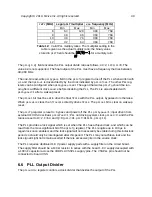
) must lie between 384–768 MHz. Table 12 summarizes the valid settings of the multiply
ratio.
Table 11:
pllcfg: PLL Configuration and Status
Copyright © 2019, SiFive Inc. All rights reserved.
29
Содержание FE310-G002
Страница 1: ...SiFive FE310 G002 Manual v19p05 SiFive Inc ...
Страница 11: ...Figure 1 FE310 G002 top level block diagram Copyright 2019 SiFive Inc All rights reserved 9 ...
Страница 15: ...Chapter 2 List of Abbreviations and Terms 13 ...
Страница 23: ...Chapter 4 Memory Map The memory map of the FE310 G002 is shown in Table 4 21 ...

