• MUL, MULH, MULHU, and MULHSU have a 5-cycle result latency.
• DIV, DIVU, REM, and REMU have between a 2-cycle and 33-cycle result latency, depending
on the operand values.
The pipeline only interlocks on read-after-write and write-after-write hazards, so instructions
may be scheduled to avoid stalls.
The E31 implements the standard Multiply (M) extension to the RISC‑V architecture for integer
multiplication and division. The E31 has a 8-bit per cycle hardware multiply and a 1-bit per cycle
hardware divide. The multiplier can only execute one operation at a time and will block until the
previous operation completes.
The hart will not abandon a Divide instruction in flight. This means if an interrupt handler tries to
use a register that is the destination register of a divide instruction the pipeline stalls until the
divide is complete.
Branch and jump instructions transfer control from the memory access pipeline stage. Correctly-
predicted branches and jumps incur no penalty, whereas mispredicted branches and jumps
incur a three-cycle penalty.
Most CSR writes result in a pipeline flush with a five-cycle penalty.
The E31 data memory system consists of a DTIM. The access latency from a core to its own
DTIM is two clock cycles for full words and three clock cycles for smaller quantities. Misaligned
accesses are not supported in hardware and result in a trap to allow software emulation.
Stores are pipelined and commit on cycles where the data memory system is otherwise idle.
Loads to addresses currently in the store pipeline result in a five-cycle penalty.
The E31 core supports the RISC‑V standard Atomic (A) extension on the DTIM and the periph-
eral memory region. Atomic memory operations to regions that do not support them generate an
access exception precisely at the core.
The load-reserved and store-conditional instructions are only supported on cached regions,
hence generate an access exception on DTIM and other uncached memory regions.
See
The RISC‑V Instruction Set Manual, Volume I: User-Level ISA, Version 2.1
for more infor-
mation on the instructions added by this extension.
Copyright © 2019, SiFive Inc. All rights reserved.
17
Содержание FE310-G002
Страница 1: ...SiFive FE310 G002 Manual v19p05 SiFive Inc ...
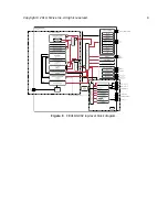
Страница 11: ...Figure 1 FE310 G002 top level block diagram Copyright 2019 SiFive Inc All rights reserved 9 ...
Страница 15: ...Chapter 2 List of Abbreviations and Terms 13 ...
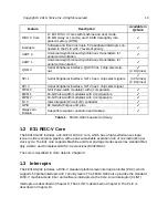
Страница 23: ...Chapter 4 Memory Map The memory map of the FE310 G002 is shown in Table 4 21 ...


