background image

Hardware Integration Guide

Rev 3  Sep.18

22

41112607

SDIO is particularly susceptible to tracking impedance and length variations between 
the SDIO tracks. Ensure that controlled impedance tracking is used, and minimize 
tracking length between the module and SD slave device. Add series resistor 
footprints at the host end to decrease the drive current and reduce potential 
interference, and match the length of all the SD tracks to within 1 mm.

SDIO tracking can cause significant radiated interference at integer multiples of the 
SD clock frequency, which can be picked up by the BX310x antenna. Bury SDIO 
tracks between ground planes and ensure stitching ground vias are placed throughout 
the board surrounding the SDIO tracking.

SDIO timing during the boot process is provided by GPIO(5) and GPIO(15). See 

Table 4-9 on page 20

 for details.

4.10 Module Enable

The AirPrime BX310x uses the ENABLE (Module Enable) signal to turn the module 
on/off:

Turn module on—Drive ENABLE high (to VDD_PADS_BB)

Turn module off—Drive ENABLE low (to 0V)

To avoid a possible implementation-dependent issue where enabling/disabling Wi-Fi 
functionality could cause a perturbation (glitch) on the power supply rails that impacts 
module operations, a short delay (1 ms recommended) is required for the power 
supply to stabilize before enabling the module.

If ENABLE is controlled by the Host, the host implements the delay (from the time the 
supply is present) before driving ENABLE high.

If ENABLE is hard-wired to the supply (VDD_PADS_BB), an RC circuit (10k

 & 

0.1uF) is required. The RC circuit will create the required delay, allowing the supply to 
stabilize before ENABLE is pulled high.

Do not leave this pin unconnected.

4.11 PWM

The AirPrime BX310x supports the use of PWM functionality on GPIOs (GPIO(5) and 
GPIO(27)) via AT command configuration. Refer to [1] AirPrime BX310x AT Command 
Reference
 for details.

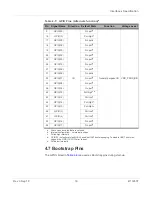
Table 4-12: Enable Pin Description

Pin

Signal Name

Direction

a

a. Signal direction with respect to the module.

Function

Voltage Level

37

b

b. Do not leave this pin unconnected.

ENABLE

I

Start/stop module VDD_PADS_BB

Содержание AirPrime BX3100

Страница 1: ...AirPrime BX3100 BX3105 Wi Fi BT Module Hardware Integration Guide 41112607 Rev 3 ...

Страница 2: ...rcraft the Sierra Wireless modem MUST BE IN AIRPLANE MODE OR POWERED OFF When operating the Sierra Wireless modem can transmit signals that could interfere with various onboard systems Note Some airlines may permit the use of cellular phones while the aircraft is on the ground and the door is open Sierra Wireless modems may be used at this time The driver or operator of any vehicle should not oper...

Страница 3: ...ark and logos are registered trademarks owned by the Bluetooth SIG Inc and any use of such marks by Sierra Wireless is under license Other trademarks are the property of their respective owners Contact Information Revision History Sales information and technical support including warranty and returns Web sierrawireless com company contact us Global toll free number 1 877 687 7795 6 00 am to 5 00 p...

Страница 4: ...Specifications 9 2 1 Features 9 3 Technical Specifications 11 3 1 Environmental 11 3 2 Power Supply Ratings 11 3 3 Power Management 11 3 4 RF 12 3 4 1 Generic Radio 12 3 4 2 Wi Fi Radio 12 3 4 3 Bluetooth Radio 13 3 5 Electrical Specifications 14 3 5 1 Absolute Maximum Ratings 14 4 Interfaces Specification 15 4 1 Overview 15 4 2 UART 15 4 3 ADC Voltage Measurement 16 4 4 I2C Interface 17 4 4 1 App...

Страница 5: ...DIO Interface 21 4 10 Module Enable 22 4 11 PWM 22 5 General Layout Recommendations 23 6 Regulatory Compliance 24 6 1 United States 24 6 2 Canada 25 7 Pinout 27 7 1 Pin Configuration 28 7 2 Pin Description 28 8 References 32 8 1 Web Site Support 32 8 2 Reference Documents 32 9 Abbreviations 33 ...

Страница 6: ... functionality into their products The following table summarizes the module s supported wireless frequencies and modes 1 2 1 Wi Fi The AirPrime BX310x supports 2 4 GHz Wi Fi operation Key features include TCP IP 802 11 b g n e i Connection methods BSS STA SoftAP Transmit power Adjustable up to 20 dBm maximum For a list of additional supported Wi Fi functionality protocols and features see Feature...

Страница 7: ...ce configuration For usage details refer to 1 AirPrime BX310x AT Command Reference available at source sierrawireless com 1 3 General Hardware Features 1 3 1 Physical Dimensions and Connection Interface AirPrime BX310x modules are compact robust fully shielded and laser marked modules with the dimensions noted in Table 1 2 The AirPrime BX310x module is an LGA form factor device All electrical and ...

Страница 8: ... Rev 3 Sep 18 8 41112607 The LGA pads have the following distribution Table 1 3 LGA Pad Types Pad Type Quantity Dimensions Pitch Signal Pads 54 outer pads 0 75x0 35 mm 0 65 mm Ground Pads 16 inner pads 1 0x1 0 mm 1 83 mm 1 48 mm ...

Страница 9: ...on TSN etc WMM PS UAPSD A MPDU A MSDU aggregation Block ACK RTS CTS ACK BA Fragmentation defragmentation CCMP CBC MAC counter model TKIP MIC RC4 WAPI SMS4 WEP RC4 CRC Frame encapsulation 802 11h RFC 1042 Pre authentication TSN Supported channels 1 14 Data transfer HTTP HTTPS MQTT TCP UDP Autoconnection After device reset automatically connects to available AP based on previous configuration Infras...

Страница 10: ...configuration UART features GATT profiles Define personal services Roles Simultaneous Central access point Peripheral client Simultaneous connections Up to 7a total simultaneous connections including up to 3a BLE connec tions Simultaneous BT Classicb and BLE connections PCMb I2Sb Configuration Device configuration methods Built in web based configuration utility See Configuration Utility on page 7...

Страница 11: ...AirPrime BX310x switches between several power modes to minimize current consumption Light Sleep and Deep Sleep modes are enabled via AT commands from the host Refer to 1 AirPrime BX310x AT Command Reference for details Table 3 1 Environmental Specifications Parameter Range Ambient Operating Temperature 40 C to 85 C Ambient Storage Temperature 40 C to 105 C Recommended Table 3 2 Power Supply Pins ...

Страница 12: ...ake the module a Available in future firmware release Table 3 4 Generic Radio Characteristics Description Min Typ Max Unit BX3100 RF Port Impedance 50 Frequency Band 2 4 2 45 2 485 GHz BX3105 Antenna Gain 0 dBi Table 3 5 Generic Radio Characteristics Description Min Typ Max Unit Transmit 802 11b CCK 1 Mbps Conducted Tx Power EVM and Mask Compliant 14 15 5 17 dBm Transmit 802 11g OFDM 6 Mbps Conduc...

Страница 13: ...5 205 band edge compliance reduction is 3 dB Table 3 5 Generic Radio Characteristics Continued Description Min Typ Max Unit Table 3 6 Generic Radio Characteristics Description Min Typ Max Unit Transmit Power BR 1 Mbps 7 5 9 10 5a a Maximum Output power is restricted by compliance to FCC 15 205 band edge to 5 5 dBm Max dBm Transmit Power EDR 2 Mbps 7 5 9 10 5 dBm Transmit Power EDR 3 Mbps 7 5 9 10 ...

Страница 14: ...H Output high voltage 0 8 VIO V Cpad Input pin capacitance 2 pF VIO VDD_PADS_BB 2 7 3 6 V IMAX GPIO maximum drive capability 12 mA TSTR Storage temperature range 40 150 C Table 3 8 Recommended Operating Conditions Parameter Min Typ Max Units VDD Supply voltage VDD_3V3_PA VDD_3V3_RF 2 3 3 3 3 6 V VIO I O supply voltage VDD_PADS_BB 2 7 3 3 3 6 V TOPR Operating temperature range 40 85 C VIL CMOS low ...

Страница 15: ...FF Table 4 1 on page 15 describes the signals used for UART0 Note UART signals are named with respect to the HOST and directions are listed with respect to the module For example UART0_RXD is an output from the module to the host The UART interface is configurable via AT commands Default configuration 115200 baudrate 8 bit no parity no handshaking Baudrate considerations Maximum supported 5 Mbaud ...

Страница 16: ...ns is read via an AT command Noise can have a large impact on sensitive voltage measurements To improve the accuracy of small voltage level measurements a100 nF capacitor to ground is recommended on the input to the VDET_1 VDET_2 SENSOR_VP and SENSOR_VN pins Access to a Hall effect sensor is supported via firmware and is selected using AT commands The sensor pins SENSOR_VP or SENSOR_VN will trigge...

Страница 17: ... transfer rates up to 400 kbit s Master mode operation Addressing modes 7 bit 10 bit Dual addressing mode External 2 2 k pull up resistors must be applied to I2 C signals see Figure 4 1 on page 17 For I2 C bus details including I2C bus waveform and timing details refer to the I2C Bus Specification 4 4 1 Application Figure 4 1 Example of I2C Bus Application Table 4 4 I2 C Interface Pinsa a Leave op...

Страница 18: ...rime BX310x defines several GPIOs for customer use as described in Table 4 6 and Table 4 7 Note The pins carrying the Alternate function GPIOs are multi function The alternate inter faces SDIO or SPI can be selected via an AT command Table 4 5 I2S Interface Pinsa a Leave open any pins that are not used Pin Signal name Directionb b Signal direction with respect to the module Function Voltage Level ...

Страница 19: ... GPIO 32 No pullb 25 GPIO 33 No pullb 26 GPIO 18 No pullb 27 GPIO 26 No pullb 31 GPIO 36 No pullb 32 GPIO 37 No pullb 34 GPIO 38 No pullb 36 GPIO 39 No pullb 42 GPIO 15 Pull highc d 43 GPIO 12 Pull lowe 44 GPIO 14 Pull highc 45 GPIO 13 Pull highc 46 GPIO 2 Pull lowe 47 GPIO 4 Pull lowe 53 GPIO 16 No pullb 54 GPIO 17 No pullb a Leave open any pins that are not used b Internal configuration no inter...

Страница 20: ... Function Alternative 0 Boot Source High Internal pull 45 k Boot from Internal Flash Download to Flash Disabled 2 Boot Source High Internal pull 45 k 5 SDIO Slave Timing High Internal pull 45 k Rising Edge Input Output See Table 4 9 15 MTDO High Internal pull 45 k 12 MTDI SDIO Interface Voltage Low Internal pull 45 k 3 3V 1 8V Not supported Table 4 9 SDIO Slave Timing Configuration GPIO 5 GPIO 15 ...

Страница 21: ...le 4 11 describes the signals used for SDIO Note The pins carrying the SDIO interface are multi function The alternate interfaces GPIO or SPI can be selected via an AT command 45 HSPID MOSI O I MOSI 46 HSPIWP O Write Protect M 47 HSPIHD SRDY O O Hold a Leave open any pins that are not used b Signal direction with respect to the module Table 4 11 SDIO Pin Descriptionsa a Leave open any pins that ar...

Страница 22: ...ff Turn module on Drive ENABLE high to VDD_PADS_BB Turn module off Drive ENABLE low to 0V To avoid a possible implementation dependent issue where enabling disabling Wi Fi functionality could cause a perturbation glitch on the power supply rails that impacts module operations a short delay 1 ms recommended is required for the power supply to stabilize before enabling the module If ENABLE is contro...

Страница 23: ... plenty of ground vias throughout the application board Tightly tie ground planes together throughout the application board BX3100 RF tracking to application board antenna or RF connector Use 50 impedance controlled tracks Do not track near sources of digital interference Provide continuous unbroken ground plane reference Avoid multiple layer changes Supply decoupling should be placed as close to ...

Страница 24: ...als may be obtained upon customer request contact your Sierra Wireless account representative for details Additional testing and certification may be required for the end product with an embedded BX3100 BX3105 module and are the responsibility of the OEM Sierra Wireless offers professional services based assistance to OEMs with the testing and certification process if required 6 1 United States Th...

Страница 25: ...een approved by Innovation Science and Economic Development Canada to operate with the antenna types listed below with the maximum permissable gain indicated Antenna types not included in this list that have a gain greater than the maximum gain indicated for any type listed are strictly prohibited for use with this device Integrators may use the BX3100 BX3105 modules in their end products without ...

Страница 26: ... aux CNR d Industrie Canada applicables aux appareils radio exempts de licence L exploitation est autorisée aux deux condi tions suivantes 1 l appareil ne doit pas produire de brouillage et 2 l utilisateur de l appareil doit accepter tout brouillage radioélectrique subi même si le brouil lage est susceptible d en compromettre le fonctionnement 5 A user manual with the end product must clearly indi...

Страница 27: ...nly these functions and associated pins is guaranteed to be forward and or backward compatible with the next generation of CF3 modules Extension functions and associated pins Bring additional capabilities to the customer Whenever an Extension function is available on a module it is always at the same pin location Custom functions and associated pins These are module specific and make use of specif...

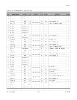
Страница 28: ...on for the LGA pins Important Leave open all pins that are not used Table 7 1 Pin Definitions Pin Signal name Group I Oa Voltage PU PDb Activec Function Typed 1 Reserved NoConnect E 2 UART0_RTS_GPIO 22 UART0 I VDD_PADS_BB PU L UART0 Request To Send C 3 UART0_CTS_GPIO 19 UART0 O VDD_PADS_BB PU L UART0 Clear To Send C 4 UART0_TXD UART0 I VDD_PADS_BB PU L UART0 Transmit Data C 5 UART0_RXD UART0 O VDD...

Страница 29: ... voltage measurement C GPIO 34 GPIO I O NP SW General Purpose I O 19 VDET_2 VoltMeasure I VDD_PADS_BB NP H ADC input for voltage measurement C GPIO 35 GPIO I O NP SW General Purpose I O 20 Reserved NoConnect C 21 Reserved NoConnect C 22 Reserved NoConnect C 23 Reserved NoConnect C 24 I2S_DO I2S O VDD_PADS_BB PD H I2S Data Out C GPIO 32 GPIO I O NP SW General Purpose I O 25 I2S_DI I2S I VDD_PADS_BB...

Страница 30: ...erved NoConnect E 39 GND Ground 0V 0V Ground C 40 RF_MAIN RF I O BX3100 RF antenna DC blocked BX3105 Leave pin unconnected C 41 GND Ground 0V 0V Ground C 42 SD_CMD SDIO I O VDD_PADS_BB NP H SDIO Command E HSPICS0 SPI I O NP SW SPI Chip Select C GPIO 15 GPIO I O NP SW General Purpose I O E 43 SD_DATA2 SDIO I O VDD_PADS_BB NP H SDIO Data bit 2 E HSPIQ SPI I O NP SW SPI Data In C GPIO 12 GPIO I O NP ...

Страница 31: ...7 Min 3 3V Typ 3 6 Max 3 3v nominal supply for Baseband and Digital I O C 53 GPIO 16 GPIO I O VGPIO NP SW General Purpose I O C I2C2_SDA I2C2 I O PUE L Primary I2C interface Data 54 GPIO 17 GPIO I O VDD_PADS_BB NP SW General Purpose I O C I2C2_SCL I2C2 I O PUE L Primary I2C interface Clock G1 G16 Ground Ground 0V 0V Ground C a I O Signal direction with respect to the module b PU PD NP No Pull PD P...

Страница 32: ...e sierrawireless com for the latest documentation available for the AirPrime BX310x 8 2 Reference Documents 1 AirPrime BX310x AT Command Reference Reference number 41111445 2 The I2C Bus Specification Version 2 1 January 2000 Phillips Semiconductor document number 9398 393 40011 ...

Страница 33: ... General Access Profile GATT General Attribute Profile HTTP Hypertext Transfer Protocol HTTPS Hypertext Transfer Protocol Secure LE Low Energy MQTT Message Queuing Telemetry Transport PAN Personal Area Network RFCOMM Radio Frequency Communication SDP Service Discover Protocol SMP Security Manage Protocol SPP Bluetooth Serial Port Profile STA Station client UART Universal Asynchronous Receiver Tran...

Отзывы: