13
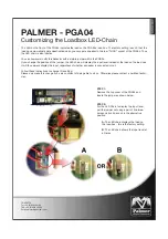
Figure 17: PCB2 jumpers
A. Capacitor discharge switch
B. J1 - jumper 1, pins 1-2
C. J2 - jumper 2, pins 1-2
D. J3 - jumper 3, pins 1-2
E. J4 - jumper 4, pins 1-2
1
2
1
2
3
Pin position
Pin position
Hazardous voltage.
Could result in serious injury or equipment malfunction.
For maintenance work, the toggle switch (58) on PCB2 must be in the
"discharge capacitors" position (position I). Do not work on the
capacitor circuits when the red discharge LED is lit.
For normal operation, the toggle switch (58) on PCB2 must be in the
"operating" position (O).
3
Discharge switch for the capacitors
The discharge switch on the switch unit driver
(SUD) module/printed circuit board PCB2
serves to discharge the capacitors. In the
“discharge capacitors” position (I), the
capacitor charging operation is turned off and
the capacitors are discharged via a resistor –
discharge of the capacitors takes roughly one
minute.
When capacitors are charged and the switch
is changed from the “operating position” (O)
to the “discharge capacitors” (I) position, the
red LED next to switch illuminates.
When the discharging has reached a safe limit
with a capacitor voltage below approximately
40 V, the LED no longer illuminates. Work on
the capacitor circuits should only be
performed once the LED no longer
illuminates.
For normal operation, the switch must be
brought into the “operating” position (O) as
shown in Figure 17: PCB2 jumpers. In this
position, the capacitors will be charged. The
LED does not light up during normal
operation.
A
B
C
D
E
B
C
D
E
Содержание SDR 15.5
Страница 39: ...39 ...


