Copyright © Siemens AG 2016. All rights reserved
162
ERTEC 200P-2 Manual
Technical data subject to change
Version 1.0
2.3.5.4 EMC Notes
2.3.5.4.1 Remapping
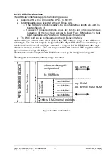
Remapping the AHB address range from 0x0000_0000 to 0x0FFF_FFFF to the range of
the SDRAM or the flash/SRAM block. This is required for some masters (ARM CPUs)
because their exception table is expected when you boot at address 0x0000_0000.
The address may be moved from 0 to another address range depending on the
MEM-
SWAP
signal.
"00"
no action (
Default
: Boot ROM)
"01" start address of SDRAM device (sub-range #1)
"10" start address of Asynchronous device (sub-range #2)
"11" no action (QVZ error upon access to 0x0000_0000, see 2.3.2.5.1)
There is no address remap with 00 or 11. With 01, address 0x0000_0000 is forwarded to
the start address of the SDRAM. With 10, address 0x0000_0000 is forwarded to the start
address of the asynchronous RAM, ROM or flash. In the latter two cases, address con-
version is carried out so that the required memory can be reached.
If, for example, the exception table of a CPU is located in the flash memory (sub-
range#2), an ARM-CPU requires this table at 0x0000_0000 during booting. The address
is therefore remapped (in line with
MEM_SWAP
).
In order to avoid unnecessary wait states at the AHB bus, the EMC can buffer a maxi-
mum of 4 instances of AHB write access and acknowledge them immediately (provided
there are no more than 4). Read access is delayed until the write buffer is empty (all data
have been written).
2.3.5.4.2 Maximum number of wait cycles
The configured value for the maximum number of wait cycles should be configured at
least 5 times bigger than the expected worst case delay time of the external wait signal.
False QVZ interrupts are possibble when the number of wait cycles and the delay of the
external wait signal have the same size. There is no way to detect a false QVZ interrupt
by software but to compare a read value with an expected value. If a false QVZ interrupt
is generated then the stored QVZ address can be false, too.
2.3.5.4.3
Shift Mode with the Asynchronous EMC Interface
Irrespective of the configuration of the boot pins, i.e. in every boot mode, the asynchro-
nous EMC interface (CS0 – CS3) is configured in shift mode so that a max. address
range of 64 MByte can be addressed per chip select. The
EXTENDED_CONFIG.ASYNC_ADDR_MODE bit is set in the EMC interface by the pri-
mary boot loader (see 2.3.1.5.1).
This parameter assignment allows you to address:
16 MByte with a data bus width of 8 bits (byte)
32 MByte with a data bus width of 8 bits (byte)
64 MByte with a data bus width of 32 bits (word)
.
Содержание ERTEC 200P
Страница 1: ...ERTEC 200P 2 Enhanced Real Time Ethernet Controller Manual ...
Страница 309: ...Copyright Siemens AG 2016 All rights reserved 309 ERTEC 200P 2 Manual Technical data subject to change Version 1 0 ...
Страница 492: ...Copyright Siemens AG 2016 All rights reserved 492 ERTEC 200P 2 Manual Technical data subject to change Version 1 0 ...

