– 1 –
MD-M3/M1
CONTENTS
MD-M3
SERVICE MANUAL
SHARP CORPORATION
No.S6940MDM3M1//
• In the interests of user-safety the set should be restored to its original
condition and only parts identical to those specified should be used.
This document has been published to be used
for after sales service only.
The contents are subject to change without notice.
Page
IMPORTANT SERVICE NOTES (FOR U.S.A. ONLY) ........................................................................................................ 2
SPECIFICATIONS .............................................................................................................................................................. 3
NAMES OF PARTS ........................................................................................................................................................... 4
OPERATION MANUAL ....................................................................................................................................................... 7
QUICK GUIDE .................................................................................................................................................................... 9
DISASSEMBLY ................................................................................................................................................................ 11
REMOVING AND REINSTALLING THE MAIN PARTS ................................................................................................... 13
TEST MODE .................................................................................................................................................................... 15
ADJUSTMENT ................................................................................................................................................................. 17
EEPROM WRITING PROCEDURE .................................................................................................................................. 23
EXPLANATION OF MECHANISM ERROR ...................................................................................................................... 24
EXPLANATION OF ERROR DISPLAY ............................................................................................................................. 25
NOTES ON SCHEMATIC DIAGRAM .............................................................................................................................. 26
TYPE OF TRANSISTOR AND LED ................................................................................................................................. 26
BLOCK DIAGRAM ........................................................................................................................................................... 27
SCHEMATIC DIAGRAM / WIRING SIDE OF P.W.BOARD ............................................................................................. 32
WAVEFORMS OF CD CIRCUIT ...................................................................................................................................... 54
WAVEFORMS OF MD CIRCUIT ..................................................................................................................................... 55
TROUBLE SHOOTING (CD SECTION) .......................................................................................................................... 57
TROUBLE SHOOTING (MD SECTION) ........................................................................................................................... 61
TROUBLE SHOOTING (POWER SUPPLY SECTION) ................................................................................................... 65
FUNCTION TABLE OF IC ................................................................................................................................................ 66
REPLACEMENT PARTS LIST/EXPLODED VIEW/PACKING OF THE SET (FOR U.S.A.)
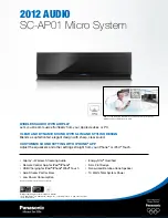
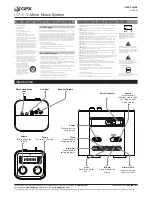
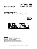
MD-M3 MD micro System consisting of
MD-M3(main unit) and CP-M3(speaker
system).
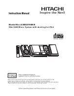
MD-M1 MD micro System consisting of
MD-M1(main unit) and CP-M1(speaker
system).
Illustration: MD-M3
Illustration: MD-M1
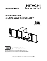
MD-M1
Содержание CP-M1
Страница 74: ...MD M3 M1 74 MEMO ...