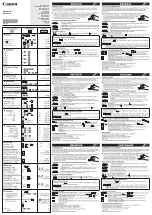
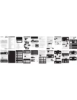
manualshive.com logo in svg
background image

Notes

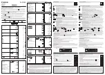
 Gate symbols and signal names are presented in accordance with:

 logic 1  =  GND
 logic 0  =  V–24

The symol 

N

cp

 denotes a physical connector pin, where 

c=connector and p=pin. Solid black end is the male side of 

the connector. White end is the female side of the connector.


 connection between different sections.


 connection limited to same section.

      Arrows indicate direction of signal or energy flow.

 The symbol     without an additional label denotes VDD (–24V).

 Capacitance in microfarads unless otherwise indicated.

 This schematic includes the user memory which is not present in the Compet 17 model. Components marked with “§” 

are not present in the Compet 17.

 These drawings based on a Model CS-17C unit with Serial No. 810591T.

Log

 2000 Jul:

Initial drawing / bhilpert.

 2004 Oct:

Signals on the remote connector (NR) elaborated further.
Switches and notes about single-cycle control of P added.

 2017 May:

Format updates.  Question of pins on IC 5-6 noted.
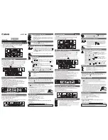
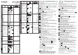
 Gate Identification

Gates and logic elements are identified by symbols of the following form:

Gate ID

                                         Description                                         

1-

n

inverter

in µPD1 IC

2-

n

2 by 2 AND–OR gate in µPD2 IC

3-

n

4-input AND gate

in µPD3 IC

4-

n

flip-flop

in µPD4 IC

5-

n

4-bit shift register

in µPD5 IC

6-

n

8-bit shift register

in µPD6 IC

7-

n

MOSFET

in µPD7 IC

M-

n

MOSFET

discrete

Discrete gates have no distinguishing identifier but their inputs are identified with a label indicating the location of the 

diode which implements it:

Label

                                         Description                                         

g.p

diode in TDA001 or TDA002 package 

g at pin p

d

n

discrete diode

See the IC Pinouts and Gate Construction page for more about the integrated circuits.

See the Physical Layout and Connectors page for more about IC and gate location.

Sharp  Compet  17  Calculator

Section: Notes

 Page: 2

Rendition: 2020 May 20
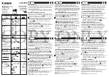
Signal Names

Section

Signal

Description

Timing

Ø…

Master timing.

Ø1

Master clock, data capture phase.

Ø2

Master clock, output transition phase.

Ø3

Master clock, a third phase used by some flip-flops.

ØB…

Bit timing.

ØD…

Digit timing (4 bits constitutes a digit).

ØnB1+3

Used for triggering digit timing and display latch.

Øn(D16•B8•1)

Capture pulse at the end of each full number cycle.

Keyboard

K…

The keyboard and numeral encoder.

P

Indicates a number cycle during which processing occurs.

Control

S…, C…

The state machine.

C

Multiply or divide operation pending.

D

Divide operation pending.

F, G, J, M, S

Assorted state flags.

S…

Assorted internal state signals.

IDLE

1 during display and simple operations, 0 during multi-cycle operations.

CX…

Outputs from control to the X register.

CW…

W register.

CM…

M register.

CPX…

PX decimal point counter.

CPW…

PW decimal point counter.

CPY…

PY digit counter.

X Register

X…

The operand being displayed. Arithmetic is also incorporated in this register.

XC1,2,4,8

BCD numerals on their way to the display.

CARRY

Carry indication to control.

W Register

W

The second operand.

M Register

M

The user memory.

PX Counter

PX

Ring counter to hold the place of the decimal point for the X operand.

PXI

Signal to the display to turn on the decimal point at the appropriate time.

PW Counter

PW

Ring counter to hold the place of the decimal point for the W operand.

PY Counter

PY

Ring counter used during multiply and divide operations.

A lowercase “n” in a symbol name indicates the logical NOT operation.

The character  “ • ”  in a symbol name indicates the logical AND operation.

The character  “+”  in a symbol name indicates the logical OR operation.

P-Cycles and Manual Control of Operations

Two switches can be plugged into the remote connector (NR) to provide the ability to single-step through the 

major state cycles of an operation. See the Keyboard page for wiring of the switches.

A P-cycle is a full number cycle during which processing occurs and is indicated by the P signal. Major state 

transitions occur at the end of a P-cycle. Simple user operations such as numeral entry generate a single P-cycle 
without sending IDLE to 0. More complex operations requiring multiple number cycles generate a first P-cycle 
and send IDLE to 0. Multiple P-cycles are subsequently generated until the operation is complete, at which time 
IDLE returns to 1. 

Enabling the MANUAL switch disables the automatic generation of P-cycles for multi-cycle operations. In this 

mode, once a multi-cycle operation has been initiated, each press of the STEP pushbutton generates a single 
P-cycle, so the operation can be stepped through one P-cycle at a time.

Содержание Compet 17

Страница 1: ...Outputs 9 Registers 10 Arithmetic 11 Decimal Point Counters 12 Display 13 Power Supply 14 Timing Diagram 15 IC Pinouts Gate Construction 16 Physical Layout and Connectors 17 Sharp Compet 17 Calculator Sharp Compet 17 Calculator Section Title and Contents Page 1 Rendition 2020 May 20 This schematic has been derived through reverse engineering This is not the manufacter s schematic nor is it based o...

Страница 2: ...e pulse at the end of each full number cycle Keyboard K The keyboard and numeral encoder P Indicates a number cycle during which processing occurs Control S C The state machine C Multiply or divide operation pending D Divide operation pending F G J M S Assorted state flags S Assorted internal state signals IDLE 1 during display and simple operations 0 during multi cycle operations CX Outputs from ...

Страница 3: ... bits VCL Keyboard Control CARRY Arithmetic BCD serial adder 4 bits C Flag D Flag M Flag S Flag F Flag J Flag G Flag State Sequencing S1 S6 CX CA CB X Outputs 1 of 10 Decoder and Drivers Timing Numeral Encoder K0 K9 KNUM M W X KNDP Decimal Point Driver logic supplies display supplies V 90D V 90 V 190 Power Supply 000987654321 Decimal Point PX Ring Counter Ø3 XC1 XC2 XC4 XC8 W X CSUB CTC Arithmetic...

Страница 4: ... 3 B Q3 2 B Q4 1 B ØnB1 3 ØnB4 5 3 D1 ØT 7 6 ØC 8 Q1 4 B Q2 3 B Q3 2 B Q4 1 B ØnB1 3 ØnB4 5 4 D1 ØT 7 6 ØC 8 Q1 4 Q2 3 Q3 2 Q4 1 ØnD2 ØnD3 NL40 ØnD4 NL38 ØnD5 NL42 ØnD6 ØnD7 NL44 ØnD8 ØnD9 ØnD10 ØnD11 NL11 ØnD12 NL9 ØnD13 NL7 NL17 8 4 1 1 2SC458 1K ØnB1 3 100K Ø3 B B B B 2SC458 15K NL5 ØnD1 NL15 ØnD2 ØnD3 ØnD4 ØnD5 ØnD6 ØnD7 ØnD8 ØnD9 ØnD10 ØnD11 ØnD12 ØnD13 7 5 1 2 ØD1416 NL6 ØnD16 NL16 10 2 1 6 ...

Страница 5: ...95 96 96 96 96 94 94 94 93 93 93 92 92 92 KNUM 3 1 Ø2 4 6 D Q ØT 2 10 5 ØC 11 Ø3 ØR 1 7 5 1 7 KCLR E D Øn D16 B8 1 7 12 2 Ø2 4 6 D Q ØT 3 9 ØC Ø3 ØR E Øn D16 B8 1 4 1 7 12 5 Ø2 4 6 D Q ØT 4 8 5 ØC 7 Ø3 ØR 1 E Øn D16 B8 1 nP P 0 047 100K E E NK40 E D D D D D D IDLE 300K VCL 98 4 98 3 98 2 98 1 91 1 91 2 91 3 91 4 97 1 97 2 97 3 97 4 d45 d30 d29 d46 d31 d26 d27 d28 d42 d33 d32 NR40 NK35 NK27 IDLE nD...

Страница 6: ... 7 14 7 8 KEQ nC D 7 14 2 3 KEQ nC nD 8 4 1 3 D KEQ C nD 4 7 5 1 3 D 7 12 10 9 KNP nM nS KNP 7 13 10 9 KS nC nD KS 11 KMD KCLR S2 nF J nM K 67 4 S2 nF J nM K KCLR 67 67 1 67 2 67 3 68 4 68 68 1 68 2 68 3 25 2 KRC KEQ KNP nM nS 25 25 3 25 4 14 4 S2 F J 25 1 KNDP M S M 8 KMR 16 1 KCLR KMD S KMAS 16 16 2 16 3 16 4 S2 nF J nM 17 1 S2 nF J nM KMS 17 17 3 17 4 17 2 27 3 KRC KMD S KEQ 27 27 1 27 4 27 2 K...

Страница 7: ... 3 3 11 10 8 9 ØnD16 ØB8 W E 7 2 8 4 3 1 2 Øn D16 B8 1 5 PX 9 3 1 4 nG G D G nG 7 5 1 4 nF D nF nJ nF J F nJ F J M 5 E KCLR 7 12 7 8 11 KNP F nF nF nF J J Ø1 15 1 S3 KEQ nC D S6 nF nJ 23 15 2 15 3 15 4 KDP S4 nF nJ S1 nF J M 13 4 23 1 23 2 S6 nF J 23 3 S5 nF J KEQ C D S1 nF J nM 23 4 33 1 58 2 MUL M nS d6 MUL nM nS 22 1 S6 F J S4 F J SCa 22 22 2 22 3 22 4 KEQ S2 F J S2 F nJ 26 1 26 2 26 3 KCE 26 4...

Страница 8: ... 5 D Q ØT 4 8 5 ØC 7 Ø3 ØR 1 E CPA 7 9 J 2 3 1 S1 nJ 7 9 5 4 7 9 10 9 11 7 9 7 8 S1 nF J nM 7 11 10 9 11 7 11 7 8 S2 nF J nM Ø2 4 5 D Q ØT 3 9 ØC 11 Ø3 ØR E CPA 7 10 5 4 1 7 10 2 3 7 10 7 8 11 7 10 10 9 Ø2 4 5 D Q ØT 2 10 ØC Ø3 ØR E CPA S3 H IDLE to P generator KEQ nC D KEQ C D S4 F J 12 1 12 12 3 12 4 12 2 K K S2 F nJ K K S2 nF J M KEQ nC nD d16 d44 K S6 nF J 38 3 42 1 K K K K K K KEQ C nD C D S2...

Страница 9: ...KMD S CPWØnG 57 4 SCh KNDP M S nC nD KCLR KMD S K S5 F J SCf 44 1 45 1 35 4 CPWPX CXØD11 SCm SCf SCg MUL nM nS S2 nF nJ KCE S2 F J SCc SCm K SCg S1 F J 48 1 49 1 32 1 CTC K CWW SCm MUL M nS 31 2 58 3 35 2 SCh KNDP M S nC nD KCLR KMD S 66 66 1 66 2 66 3 SCf 32 2 SCm CWØ 66 4 MUL nM nS K M 2 G S6 nF J D1 G D2 13 2 SCk S1 nF J M K 14 3 37 2 d17 S2 F J CMØ KMC 24 4 SCa SCm SCe 41 31 4 41 1 41 2 nP KNP...

Страница 10: ... ØT 6 7 ØC Ø3 ØR Ø2 6 2 DA1 QA8 ØT 8 9 3 ØC 4 Ø3 ØR 2 Ø2 6 2 DB1 QB8 ØT 6 7 ØC Ø3 ØR Ø2 6 1 DA1 QA8 ØT 8 9 3 ØC 4 Ø3 ØR 2 Ø2 6 1 DB1 QB8 ØT 6 7 ØC Ø3 ØR W E CWW 2 1 3 4 1 2 CWX X 5 E 2SC458 5K 4 5 7 5 MØ CPM Ø2 6 6 DA1 QA8 ØT 8 9 3 ØC 4 Ø3 ØR 2 Ø2 6 6 DB1 QB8 ØT 6 7 ØC Ø3 ØR Ø2 6 5 DA1 QA8 ØT 8 9 3 ØC 4 Ø3 ØR 2 Ø2 6 5 DB1 QB8 ØT 6 7 ØC Ø3 ØR Ø2 6 4 DA1 QA8 ØT 8 9 3 ØC 4 Ø3 ØR 2 Ø2 6 4 DB1 QB8 ØT 6...

Страница 11: ... 3 D Q1 4 D XC4 XC3 XC2 XC1 3 1 ØB8 CTC 4 1 3 2 5 E E CARRY H 7 3 11 7 9 8 10 H Ø2 4 1 D Q ØT 4 8 ØC Ø3 ØR E 2 1 9 8 10 11 7 E Ø1 ØnB8 H 7 4 1 3 5 2 4 CSUB Six Generator Tens Carry Detector Carry Latch Operand Adder CSUB 7 3 1 2 4 3 5 7 2 11 8 10 7 9 7 2 1 2 4 3 5 Normalisation Adder Sum H 8 7 4 E 9 10 7 11 Ø1 XØ 11 1 1 6 D CSUM ØnD1 A In B In Normalisation Carry Latch Check pin numbers and orderi...

Страница 12: ... ØT 2 10 5 ØC 11 Ø3 ØR 1 CPXØnD13 2 7 1 2 3 4 5 CPXØD13 7 5 1 5 ØnD13 ØD13 nP 11 1 1 7 nPXI NL35 NK8 PW ØD13 Ø2 6 11 DA1 QA8 ØT 8 9 3 ØC 4 Ø3 ØR 2 Ø2 6 11 DB1 QB8 ØT 6 7 ØC Ø3 ØR E PW E CPWPW 2 6 3 4 1 2 CPWPX PX 5 CPWPY 2 6 11 10 9 8 CPWDPØD DPØD 7 PY 2SC458 5K cpw CPWØG 2 11 9 8 11 10 7 CPWØnG 9 3 1 5 G nG 2SC458 5K ØnB8 Ø1 83 nP cpy Ø2 6 10 DA1 QA8 ØT 8 9 3 ØC 4 Ø3 ØR 2 Ø2 6 10 DB1 QB8 ØT 6 7 Ø...

Страница 13: ... 2SC857 110K 2SC857 110K 2SC857 110K 2SC857 110K 2SC857 110K 2SC857 110K 2SC857 10K 2SC458 10K 10K 2SC458 10K 10K 2SC458 10K 10K 2SC458 10K 9 3 1 2 XC2 NL2 9 10 7 1 n4 4 10 2 1 2 XC3 NL1 3 2 7 1 n8 8 11 1 1 2 XC4 NL3 4 5 7 1 8 4 1 2 XC1 NL4 10K 2SC458 10K 2SC857 1K n4 n8 2 n4 n2 4 2 4 1S84 ØnB1 3 6 2SC458 40K 2SC458 ØnD1 ØnB1 3 110K 2SC458 20K 20K 50K 200pF Ø3 40K 11 ØnD1 ØnB1 3 b b 1 B B A A A A ...

Страница 14: ...pF red blue 20 35V 1K 1W 10 315V NM11 NM10 NM6 NM5 NM3 NP2 VDD 0 047 250V 3K 1K NL29 NL30 17V NL27 NL28 NL31 NL32 brown grey white 9 10 9 7 5 7 8 7 13 Unused Elements NK42 µPD7 6 12 ØnB1 3 2 1 2 2 2 3 2 4 2 5 2 6 2 7 2 8 2 9 2 10 2 11 2 12 3 1 3 2 3 3 1 1 1 2 1 3 1 4 1 5 1 6 1 7 4 1 4 2 4 3 4 4 4 5 4 6 4 7 5 1 5 2 5 3 5 4 5 5 5 6 6 1 6 2 6 3 6 7 6 8 6 9 6 4 6 5 6 6 6 10 6 11 6 12 7 2 7 3 7 4 7 5 7...

Страница 15: ...1 9 KHz ØB1 ØB2 ØB4 ØB8 744 Hz ØnD1 ØnD2 ØnD16 16 1 PXI 80 120 160 200 240 280 320 360 400 440 480 520 560 2 3 4 5 6 7 8 9 10 11 12 13 14 X One full number cycle in registers Digit being displayed ØDn 1 LSD 2 3 4 5 6 7 8 9 10 11 12 MSD ØnB1 3 600 640 0µS 15 16 X and PXI with 000987654321 in the display logic 0 24V logic 1 0V GND ...

Страница 16: ...VDD D 50K to VDD E 100K to VDD H 150K to VDD J 300K to VDD K 300K to VCL nn 470K to VCL internal to TDA002 unit nn a 40K to GND b 60K to GND c 100K to GND d 300K to GND Occasionally individual MOSFET transistors or MOSFETs contained in µPD7 ICs are used as AND gates The gate of these transistors functions as an inverted input Because the MOSFET is a bidirectional device a diode is usually required...

Страница 17: ...mponent side view NP01 NP06 1 1 5 5 5 4 5 3 5 2 5 1 1 2 7 1 Sharp Compet 17 Calculator Section Physical Layout and Connectors Page 17 Rendition 2020 May 20 03 04 05 01 Italicised expressions are connections with no signal name in the schematic ØnDx signals on the NK and NR connectors have a diode between the connector and the actual signal See the Keyboard page The NK and NR connector pins are num...

Отзывы: