


11
26PL83M
Ë
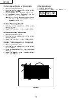
MTS ADJUSTMENT
MTS Level Adjustment
1. Receive the following composite signal.
Monaural signal: 400Hz, 100% modulation
2. Connect the rms voltmeter to pin (39) of IC3001.
3. Enter the service mode and select the service
adjustment "M01" and set to "09".
4. Enter the service mode and select the service
adjustment "EX4".
5. Adjust the data so that the rms voltmeter reads 490
±10 mVrms.
MTS VCO Adjustment
1. Keep the unit in no-signal state.
2. Connect the frequency counter to pin (39) of IC3001.
3. Connect a capacitor (100µF, 50V) in between
po) side of C3005 and ground.
4. Enter the service mode and select the service
adjustment "M02"
5. Adjust the data so that the frequency counter reads
62.94 ±0.75kHz.
Filter Adjustment
1. Feed the following stereo pilot signal to pin (14) of
IC3001 .
Stereo pilot signal: 9.4kHz, 600mVrms.
2. Enter the service mode and select the service
adjustment "M03".
3. Adjust the data until "OK" appears in position on the
screen. Make sure the "OK" is displayed almost at
the center of the data range.
Separation Adjustment
1. Connect the rms voltmeter to pin (39) of IC3001.
2. Receive the following composite stereo signal 1.
Composite stereo signal: 30% modulation, left
channel only, noise reduction on, 300Hz
3. Enter the service mode and select the service
adjustment "M04".
4. Adjust the data until the AC voltage reading of the
RMS voltmeter is minimum.
5. Receive the following composite stereo signal 2.
Stereo signal: 30% modulation, left channel only,
noise reduction on, 3kHz
6. Enter the service mode and select the service
adjustment "M05".
7. Adjust the data until the AC voltage reading of the
rms voltmeter is minimum.
8. Take the above steps 1 thru 7 again for fine
adjustment.
Содержание 26PL83M
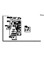
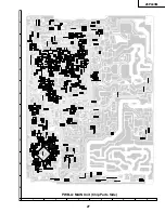
Страница 12: ...13 26PL83M 12 12 11 10 9 8 7 6 5 4 3 2 1 A B C D E F G H CHASSIS LAYOUT ...
Страница 13: ...14 6 5 4 3 2 1 A B C D E F G H 26PL83M BLOCK DIAGRAM ...
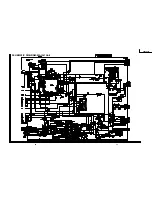
Страница 15: ...17 26PL83M 16 12 11 10 9 8 7 6 5 4 3 2 1 A B C D E F G H SCHEMATIC DIAGRAM MAIN 1 Unit ...
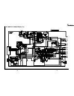
Страница 16: ...19 26PL83M 18 12 11 10 9 8 7 6 5 4 3 2 1 A B C D E F G H SCHEMATIC DIAGRAM MAIN 2 Unit ...
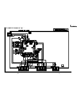
Страница 17: ...21 26PL83M 20 12 11 10 9 8 7 6 5 4 3 2 1 A B C D E F G H SCHEMATIC DIAGRAM AV Unit ...
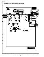
Страница 18: ...22 6 5 4 3 2 1 A B C D E F G H 26PL83M SCHEMATIC DIAGRAM CRT Unit ...
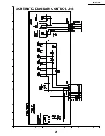
Страница 19: ...23 6 5 4 3 2 1 A B C D E F G H 26PL83M SCHEMATIC DIAGRAM CONTROL Unit ...
Страница 20: ...24 6 5 4 3 2 1 A B C D E F G H 26PL83M SCHEMATIC DIAGRAM MTS MODULE Unit ...
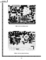
Страница 22: ...26 6 5 4 3 2 1 A B C D E F G H 26PL83M PWB A MAIN Unit Wiring Side ...
Страница 23: ...27 6 5 4 3 2 1 A B C D E F G H 26PL83M PWB A MAIN Unit Chip Parts Side ...
Страница 24: ...28 6 5 4 3 2 1 A B C D E F G H 26PL83M PWB C AV Unit Chip Parts Side PWB C AV Unit Wiring Side ...
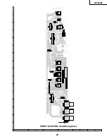
Страница 25: ...29 6 5 4 3 2 1 A B C D E F G H 26PL83M PWB F CONTROL Unit Wiring Side ...


