background image

– 20 –

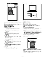
5. CMOS Black Point And White Point Defect Detect

Adjustment In Lighted

Preparation:

POWER switch: ON
Setting of pattern box:

Color temperature: 3100 

±

 20 (K)

Luminance: 900 

±

 20 (cd/m

2

)

Adjusting method:

1. Set a distance of 0.5-1.0 cm between the pattern box and

the camera.

2. Double-click on the DscCalDi.exe.
3. Select “CCD Black” on the LCD “Test”, and click the “Yes”.
4. After the adjustment is completed, the number of defect

will appear.

5. Click the OK.

Camera

Pattern box

(color viewer)

3-9. Factory Code Setting

1. Check the "Factory Code" display within the Setting group.
2. 

For U.S.A., Canada and NTSC general area

If "FC_SANYO_U" does not appear, click on the "     " mark
located on the right of the "Factory Code" display BOX and
select "FC_SANYO_U".

3. 

For Europe and PAL general area

If "FC_SANYO_EX" does not appear, click on the "     " mark
located on the right of the "Factory Code" display BOX and
select "FC_SANYO_EX".

3-10. Language Setting

1. Click on the "     " mark located on the right of the

"Language" display BOX.

2. Select language. (Default is English.)
3. End "DscCal" and remove the camera before turning the

camera power OFF.

3-11. Reset Setting
Carry out reset settings after replacing CP1 board.

1. Turn on the camera.
2. Set the NORMAL mode, and press the MENU button.
3. Choose the OPTION MENU 3.
4. Choose the RESET SETTINGS, and press the SET button.
5. Select YES, and press the SET button.

3-12. The Compulsive boot starting method

1. Keep the SHUTTER button depressed while switching on

the power.

2. Connect the camera and the computer with USB cable.

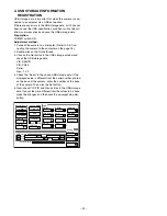
Firmware

Data

AWB

Focus

UV Matrix

R Bright

RGB Offset

Tint

B Bright

Gain

Phase

LCD

Calibration

Upload

Initialize

LCD Type

H AFC

Test

VCOMDC

VCOMPP

Cal Data

Cal Mode

OK

OK

EVF

USB storage

Get

Set

VID

Set

PID

Set

Serial

Set

Rev.

Set

Setting

Language

Video Mode

VCO

Factory Code

Hall Cal.

Backrush pulse :

Set

Get

Содержание VPC-CG20 - Full HD 1080 Video

Страница 1: ...You are requested to use RoHS compliant parts for maintenance or repair You are requested to use lead free solder This product has been manufactured using lead free solder Be sure to follow the warning given on page 2 when carrying out repair work VPC CG20 VPC CG20GD VPC CG20P VPC CG20R VPC CG20BK Product Code 168 245 02 Product Code 168 245 07 Product Code 168 245 12 Product Code 168 245 16 Produ...

Страница 2: ...0 C 662 F or less for chip compo nents to 380 C 716 F for lead wires and similar and to 420 C 788 F when installing and removing shield plates The tip of the soldering iron should have a C cut shape or a driver shape so that it can contact the circuit board as flat or in a line as much as possible Solder Use solder with the metal content and composition ratio by weight given in the table below Do ...

Страница 3: ...e The electric charges which are generated when each pixel is optically converted are in turn converted into signal voltages by the FD amplifier and they are then transmitted by the built in H driver and V driver The signals are sampled and ampli fied by the CDS and PGA circuits at the point they are output and then they are AD converted and output The output uses the 12 bit LVDS interface 1 2 3 i...

Страница 4: ...omputed from this data and three exposures are made to obtain the optimum picture The data which has already been stored in the SDRAM is read by the CPU and color genera tion is carried out Each pixel is interpolated from the sur rounding data as being either R G and B primary color data to produce R G and B data At this time correction of the lens distortion which is a characteristic of wide angl...

Страница 5: ...er or line out system DA conversion is carried out at a maximum sampling frequency of 48 kHz 4 Lens drive block 4 1 Focus drive The 16 bit serial data signals LENS_SDI and LENS_SCLK and LENS_EN which are output from the ASIC IC101 are used to drive FOCUS A FOCUS A FOCUS B and FO CUS B by the motor driver IC IC951 and are then used to microstep drive the stepping motor for focusing operation Detect...

Страница 6: ...NEL_OPEN ZCARD KEY_1ST KEY_2ND ZUSB_DET GREEN_LED RED_LED SCAN OUT0 SCAN_IN3 SCAN_IN2 SCAN_IN1 SCAN_IN0 I O I I I I O O O O I I I I I O O O I I I I Outline BOOT system reset signal 32 kHz clock input Battery OFF detection VDD1 1 VDD1 8 VDD3 VDD5 ON OFF signal SW3 2 ON OFF signal LCD panel open close detection SD card detection Key input 1st shutter Key input 2nd shutter USB detection Green LED lig...

Страница 7: ...his causes all blocks and memories other than the power sequencer of the ASIC to start operating ON OFF control for the 1 8V 2 8V and 3 3V power supplies for the CMOS sensor is carried out by the ASIC setting PAON1 and PAON2 to High or Low and also by I2C signal sent to IC501 11 Clock backup The clock backup is carried out by IC501 The ASIC gets clock information via I2C when necessary ASIC memory...

Страница 8: ...acklight system CH7 is provided to the both ends voltage of registance so that regular current can be controlled to be current that was setting 2 1 Short circuit protection circuit If output is short circuited for the length of time determined by the resister setting of IC501 all output is turned off The control signal P ON are recontrolled to restore output 3 Digital 3 25 V Power Output VDD 3 V i...

Страница 9: ...mer 1 5 Rectifier circuit The high voltage alternating current which is generated at the secondary side of T5401 is rectified to produce a high voltage direct current and is accumulated at electrolytic ca pacitor C5412 1 6 Charge monitoring circuit The functions programmed in the IC541 monitor oscillations and estimate the charging voltage If the voltage exceeds the rated value charging automatica...

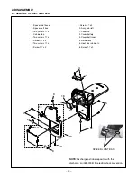
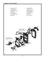
Страница 10: ...n 1 Spacer joint base 2 Spacer batt box 3 Two screws 1 7 x 4 4 Cabinet top 5 Two screws 1 7 x 6 6 Screw 1 7 x 4 7 Two screws 1 7 x 4 8 Screw 1 7 x 3 9 Screw 1 7 x 3 10 Assy cabi left 11 Cover DC 12 Cover battery 13 Cover batt inner 14 Holder lens 15 Heat sink rub heat L 16 Screw 1 7 x 2 SPACER JOINT BASE 14 15 9 16 3 4 5 10 1 8 6 12 13 2 7 11 ...

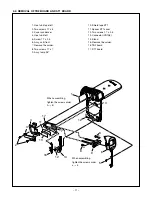
Страница 11: ...ews 1 7 x 7 9 Assy lamp SV 10 Shield tape ST1 11 Spacer ST1 cover 12 Two screws 1 7 x 3 5 13 Connector CN106 14 Stand 15 Remove the solder 16 TB2 board 17 ST1 board 2 2 REMOVAL OF TB2 BOARD AND ST1 BOARD 2 3 10 11 17 4 7 15 14 8 a b 9 6 12 16 A 8 12 13 B 1 5 When assembling tighten the screws order A B When assembling tighten the screws order a b ...

Страница 12: ... screws 1 7 x 3 5 9 Connector CN103 2 3 REMOVAL OF CP1 BOARD 10 Connector CN301 11 Unit control 12 CP1 board 13 Spacer battery 14 Heat sink rub heat L 15 Spacer lens right 16 Spacer FPC lens 17 Assy FPC CA1 SV 18 Heat sink tape top 17 2 18 15 5 3 6 10 9 4 8 13 B 14 12 8 A 7 C 16 15 1 11 When assembling tighten the screws order A B C ...

Страница 13: ...base 3 Spacer speaker wire 4 Speaker 8 5 Two screws 1 7 x 4 6 Holder speaker 7 Assy wire VF1 CP1 8 Dec bottom 9 Shield tape bottom 10 Spacer CP1 2 11 Spacer button power 12 Heat sink right 13 Shield tape bottom 14 Button power 15 Cover SD 16 Assy cabi right 2 4 REMOVAL OF ASSY CABI RIGHT When assembling tighten the screws order a b ...

Страница 14: ...Spacer MR 7 Cover joint B 8 Screw 1 7 x 2 9 Cover joint A 10 Spacer joint removed after assembly 11 Assy joint 12 Screw 1 7 x 2 13 TB1 board 14 Assy wire VF1 CP1 15 Assy magnet 16 Four screws 1 7 x 3 17 Assy COV LCD F SV 18 Connector CN171 When assembling tighten the screws order A B C D 19 LCD 20 Spacer VF 21 Two screws 1 7 x 2 22 VF1 board 23 Spacer VF1 LCD 24 Assy holder moni SV 10 9 11 10 14 1...

Страница 15: ... 15 2 6 BOARD LOCATION VF1 board TB1 board CP1 board TB2 board ST1 board ...

Страница 16: ...urn on the switch and wait for 30 minutes for aging to take place before using Color Pure It is used after adjusting the chroma meter VJ8 0192 adjust color temperature to 3100 20 K and luminosity to 900 20 cd m2 Be careful of handling the lump and its circumference are high temperature during use and after power off for a while 3 Computer screen during adjustment 3 5 Connecting the camera to the c...

Страница 17: ...nfinity 3 6 The adjustment item which in necessary in part exchange COMPL PWB CP1 Factory Cord Setting Language Setting COMPL PWB VF1 COMPL PWB ST1 COMPL PWB TB1 Reset Setting LENS Lens Adjust ment 1 m AWB Adjust ment USB storage information registration CMOS White Point Defect Detect Adjustment CMOS Black Point And White Point Defect Detect Adjustment In Lighted Be sure to carry out the necessary...

Страница 18: ...ermination is effectuated using below values The adjustment values fulfill the conditions below they are de termined as within specifications Adjustment value determination AF_TEMP_AD_I ATADI ATADI adjustment value of focus temperature A D 250 ATADI 893 PZ_BR PBR PBR adjustment value of zoom backrush pulse 0 PBR 10 AF_BR ABR ABR adjustment value of focus backrush pulse 0 ABR 10 AF_I_WIDE ZIW ZIW i...

Страница 19: ...lue of focus temperature A D 250 ATAD 893 AF_WIDE ZW ZW adjustment value of focus at zoom position wide 60 ZW 35 AF_MID1 ZM1 ZM1 adjustment value of focus at zoom position middle1 90 ZM1 20 AF_MID2 ZM2 ZM2 adjustment value of focus at zoom position middle2 78 ZM2 32 AF_TELE ZT ZT adjustment value of focus at zoom position tele 51 ZT 59 3 AWB Adjustment Preparation POWER switch ON Setting of patter...

Страница 20: ... located on the right of the Factory Code display BOX and select FC_SANYO_EX 3 10 Language Setting 1 Click on the mark located on the right of the Language display BOX 2 Select language Default is English 3 End DscCal and remove the camera before turning the camera power OFF 3 11 Reset Setting Carry out reset settings after replacing CP1 board 1 Turn on the camera 2 Set the NORMAL mode and press t...

Страница 21: ...N MENU 3 6 Choose the FORMAT 7 Toggle the SET button to the left for 2 seconds FIRMWARE UPDATE will display 8 Choose YES 9 Press the SET button Update is starting Note Do not turn off the camera s power or remove the SD card while the firmware is being updated The power will turn off after the update is complete 2 Overwriting firmware from the calibration software Preparation PC with overwriting f...

Страница 22: ...d check the USB storage data VID SANYO PID CG20 Serial Rev 1 00 4 Check the Serial in the above USB storage data If the displayed value is different from the serial number printed on the base of the camera enter the number on the base of the camera Then click the Set button 5 Next check VID PID and Rev entries in the USB storage data If any of them are different from the values in 3 above make the...

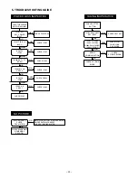
Страница 23: ...B23 KEY INPUT CHECK UNIT SW IC501 F3 PON IC502 10 PON Q5004 Gate PAON1 IC902 1 PAON2 CHECK IC101 PWA BLOCK CAA BLOCK SERIAL COMMUNICATION CHECK CP1 DMA BLOCK CHECK CP1 DMA BLOCK TAKING INOPERATIVE OFF LOW LOW NG NG ON HIGH HIGH OK OK YES HIGH OK NO LOW NG NO PICTURE MAIN CLOCK FOR SYSTEM OPERATION NO OPERATION IF ABSENT CHECK X1102 OSCILLATOR IC101 A3 XOUT CHECK OSCILLATION CHECK SOLDERING OF MEMO...

Страница 24: ...C CG20TAP VPC CG20EXBK OR 645 098 8721 CORD POWER 1 2MK VPC CG20EX VPC CG20EXGD VPC CG20EXP VPC CG20TA VPC CG20TAGD VPC CG20TAP VPC CG20EXBK OR 645 100 9708 CORD POWER 1 5MK VPC CG20EX VPC CG20EXGD VPC CG20EXP VPC CG20TA VPC CG20TAGD VPC CG20TAP VPC CG20EXBK 6 645 084 0104 CORD POWER 1 8MK VPC CG20 VPC CG20PX VPC CG20GD VPC CG20PXGD VPC CG20P VPC CG20PXP VPC CG20R VPC CG20BK OR 645 098 8714 CORD P...

Страница 25: ...25 2 1 6 3 5 4 7 ACCESSORIES SG413_ACCESSORIES ...

Страница 26: ...9 J 10 636 139 1429 SHIELD TAPE ST1 11 636 139 1412 SPACER ST1 COVER 12 636 132 1716 COMPL PWB ST 1 13 636 132 1723 COMPL PWB TB 2 14 636 133 5119 STAND SG419 J 15 636 138 5435 SPACER BATTERY SG419 J 16 636 135 2635 COMPL PWB CP 1 F W 17 636 123 5761 HEAT SINK RUB HEAT L 315 18 645 102 3285 UNIT CONTROL SG414 J 19 636 113 0752 HOLDER LENS SG214 J 20 636 123 5822 SPACER CA1 CN SG315 J 21 636 126 59...

Страница 27: ...27 2 1 6 7 14 15 16 17 13 8 9 11 10 12 18 21 20 22 19 23 17 24 23 19 5 4 3 102 101 104 105 106 107 106 108 108 108 110 111 109 103 108 105 CABINET 1 SG414 U Parts List 1 ...

Страница 28: ...G20TAP 41 636 138 9778 COVER JOINT BASE SG414 J4 VPC CG20R ONLY 42 636 133 5034 COVER JOINT A SG419 J 43 636 139 1337 SPACER JOINT SG411 J 44 636 133 5058 COVER JOINT B SG419 J 45 636 132 1297 COMPL PWB TB 1 46 636 139 4932 SPACER MR SG411 47 645 102 2899 ASSY MAGNET SG411 J 48 636 132 7879 ASSY JOINT SG411 J 49 636 131 9287 ASSY WIRE VF1 CP1 SG411 50 636 140 8462 ASSY COV LCD B SV SG414 VPC CG20R...

Страница 29: ...29 112 29 28 30 109 105 101 114 114 105 113 32 33 31 38 34 35 34 37 36 41 40 58 45 46 47 48 49 39 43 42 44 50 51 52 53 54 55 56 57 CABINET 2 SG414 U Parts List 2 ...

Страница 30: ... 409 696 2501 IC TCS10NPU IC501 410 699 0203 IC ADP50260006ACBZ BGA N S P IC504 409 702 5908 IC XC6221D502G IC901 409 696 6202 IC XC6221B082G IC902 409 690 0909 IC TK70628HC G IC903 409 690 0909 IC TK70628HC G IC951 409 701 6401 IC BU24025MWV DIODES D1901 407 261 8903 DIODE RB520S 30FJ D5071 408 069 2308 DIODE PEMG4005EJ DG 115 D5301 307 238 1206 DIODE CUS01 Q OSCILLATORS X1102 645 091 5208 OSC CR...

Страница 31: ...9502 303 338 0309 CERAMIC 0 1U K 10V C9503 303 338 0309 CERAMIC 0 1U K 10V C9504 303 338 0309 CERAMIC 0 1U K 10V C9505 303 338 0309 CERAMIC 0 1U K 10V C9506 303 338 0309 CERAMIC 0 1U K 10V C9510 303 338 0309 CERAMIC 0 1U K 10V C9511 303 276 1307 CERAMIC 1000P K 50V C9512 303 276 1307 CERAMIC 1000P K 50V RESISTOR PACKS RB101 945 037 0817 R NETWORK 0X4 1 16W RB102 945 037 0817 R NETWORK 0X4 1 16W RB...

Страница 32: ... 301 105 7902 MT GLAZE 0 000 ZA 1 16W R9001 301 225 1200 MT GLAZE 4 7K JA 1 16W R9002 301 225 1200 MT GLAZE 4 7K JA 1 16W R9003 301 226 1506 MT GLAZE 0 000 ZA 1 16W R9005 301 224 9504 MT GLAZE 2 2K JA 1 16W R9006 301 261 1509 MT GLAZE 4 3K JA 1 16W R9008 301 224 9009 MT GLAZE 10K JA 1 16W R9013 301 224 9702 MT GLAZE 22 JA 1 16W R9014 301 224 9702 MT GLAZE 22 JA 1 16W R9015 301 225 3808 MT GLAZE 1 ...

Страница 33: ... 403 473 7604 CERAMIC 10U M 6 3V C5112 403 473 7604 CERAMIC 10U M 6 3V C5201 303 408 5500 CERAMIC 2 2U K 16V C5401 303 393 2607 CERAMIC 22U M 6 3V C5410 303 428 3302 CERAMIC 0 022U K 350V C5412 404 122 4500 ELECT60U A 300V C5434 303 276 1307 CERAMIC 1000P K 50V C5435 303 286 1403 CERAMIC 10P D 50V C5436 303 381 8109 CERAMIC 1U K 6 3V RESISTOR PACK RB541 945 028 0703 R NETWORK 1KX4 1 16W RESISTORS ...

Страница 34: ...RCUIT WAVEFORMS c8 LCD CIRCUIT WAVEFORMS C8 CP1 BOARD DMA MAIN C9 CP1 BOARD TCA LENS C14 CP1 BOARD PWA POWER C15 CP1 BOARD CAA SENSOR POWER C16 CA1 BOARD IMAGE SENSOR C17 VF1 BOARD LCD CONNECTOR MIC C18 ST1 BOARD STROBE DC JACK C19 TB1 BOARD HINGE C20 TB2 BOARD BATTERY TERMINAL C20 PRINTED WIRING BOARDS P W B CA1 P W B SIDE A B C20 CP1 P W B SIDE A B C21 VF1 P W B SIDE A B C22 ST1 P W B SIDE A B C...

Страница 35: ...THE RESISTANCE WATTAGE AND VOLT AGE RATINGS SHOWN EXPLANATORY NOTES EXAMPLES Resistor 10K 1 16J means 10kilo ohm 5 1 16watt max 1M 1 10D means 1mega ohm 0 5 1 10watt max Tolerance K 10 J 5 G 2 F 1 D 0 5 Capacitor 0 047 F means 0 047micro farad Ftype Electrolytic capacitor 10 16 means 10micro farad 16volt max Inductor 330 J means 330micro henry 5 470 K means 470micro henry 10 No description J or K ...

Страница 36: ...ND 33 BAT_TEMP 34 USB_VBUS 35 CHG_CNT 36 TIMEOUT 37 ERR 38 DC_IN 39 PON 40 GND 41 UNREG 42 UNREG 43 UNREG 44 UNREG 45 UNREG 46 UNREG 47 UNREG 48 UNREG 49 GND 50 GND JW541 BROWN 1 XAN WHITE JW543 1 TRG_IN GRAY JW544 1 TRG_GND JW542 BLACK 1 XKT JW523 1 BAT_TEMP JK501 1 2 3 Z1 Z2 JW362 1 AL3 2V JW363 1 GND JW361 1 JW171 1 JW172 1 VDD3 CN171 10 C2M 4 C3P 11 VCAC 5 C3M 12 FRP 6 V_10 13 VINT1 7 V_5 14 C...

Страница 37: ... POWER SEQUN B to B SPEAKER FPC 12MHz TCA BLOCK TB2 BOARD IR UNIT CEC HPD IC191 BCLK LRCLK DACDAT I2C_ SDA SCL TMDS DDC mini HDMI UNIT SW RED GREEN _LED 1ST 2ND VREC TELE WIDE CN301 ZUSB_DET TGVD CN951 VPIXCLK SP FPC DC JACK PON VDD1 1 DC DC CONV CN651 CN191 CN543 CN901 CN912 CMOS IMAGE SENSOR 14M SD CARD SOCKET NOR FLASH MEMORY CN110 USB AV UV 0 7 Y 0 7 HDMI_INT HDMI TRANSMITTER USBD VIDEO DRIVER...

Страница 38: ...VDD3 VDD3 OUT1A OUT3A OUT1B OUT2A OUT2B OUT4B OUT4A OUT3B 4 8 5 27 25 15 17 14 44 12 42 41 39 OUT5B OUT6A OUT6B OUT5A PIOUT1 CSB STATE11 SCLK SDATA FCLK STATE21 IN5A IN5B DATA O C CONT O C EN HALL OFFSET HIREG IN HIN HIN RESETN ENABLE CLOCK IAMPPWM HALL OUT2 IRISPWM HIREG OUT PWM OUT DRIVE DRIVE HALL IN HALL IN HALL OUT HALL OUT 26 17 ZOOM_PI FOCUS_PI IC971 IRIS CONTROL IC951 LENS DRIVER ZOOM_PI_A...

Страница 39: ...2 X5001 32 768KHz HINGE CN301 SCANIN 0 4 IC121 TH301 SCANOUT 0 1 KEY_ 1ST 2ND CN106 BtoB ST1 BOARD PON DC IN NOR FLASH MEMORY HDMI TRANSMITTER SPEAKER LCD 2 7inch TB1 BOARD MIC L MIC R PAON1 PAON2 ADCK RESETN TGVD CMOS_SDA CMOS_SCL 48 00000MHz CHG FLCTL BAT_TEMP ZCHGDONE INT_TEMP STATE_ F Z ZOOM FOCUS _PI_E GRESETN VPC CG20 series only VPC CG100 series only VPC CG100 series only HALL_OUT HALL OFFS...

Страница 40: ...CHARGE SG413_ST_BLOCK CN543 TO CP1 DMA CN106 UNREG 19 18 17 16 AL3 2V ZCHGDONE FLCTL CHG POWER CIRCUIT SDA I2C_SDA SCL I2C_SCL SW1 A B C D BOOST5 3V VOUT1 A B VDD5 IC504 REG VDD EN PON SW6 VAA2 8 SWA2 A B SWB2 A B VOUT2 A B VDD3 SW3 VDD1 8 CMOS1 8 Q5003 SW PAON1 SW7 LCDAN LSTR7 LCDCA ISET7 LCDPWM VREGO AL3 2V IC501 SWITCHING CONTROL L5301 STEP UP CIRCUIT L5061 STEP DOWN CIRCUIT L5021 STEP UP DOWN ...

Страница 41: ...div 40ns div IC101 PIN AD19 EXCLKS 1V div 20µs div IC101 PIN D5 D4CKO 1V div 20ns div IC101 PIN D11 AMCLK 1V div 40ns div IC101 PIN A6 CLK12M 1V div 40ns div LCD CIRCUIT WAVEFORMS WAVEFORM TEST POINT LOCATION TEST POINT LOCATION WAVEFORM CN103 PIN 5 LCDD0 1V div 100ns div WF SG413 LCD CN103 PIN 16 LCDHD 1V div 10µs div CN103 PIN 8 LCDD3 1V div 100ns div CN103 PIN 9 LCDD4 1V div 100ns div CN103 PIN...

Страница 42: ... AL3 2V 0 1 B C1208 LCDCA TIMEOUT 0 1 B C1206 A_VDD1 8 IRISPWM 1 B 1608 C1907 220 RB127 0 1 16Z R1027 DLP2ADN900HL4 L1901 0 1 B C3010 4 7 B 1608 C1209 PON 1K 1 16J R3012 SHUTTER UP04213 Q1001 1 2 3 4 5 6 220 RB128 0 1 16Z R1018 0 1 B C1057 MIC_VDD 0 1 16Z R1005 10K RB143 10K 1 16J R1020 1 B C1102 10K 1 16J R3009 0 1 16Z R1802 C1064 0 1 B VDD3 CN103 10 LCDD5 4 HINGE 11 LCDD6 5 LCDD0 12 LCDD7 6 LCDD...

Страница 43: ...CTL ZCHGDONE ZCHGDONE 100 RB129 1 2 EXCLKS USB_5VON 3 4 G_EN A_VDD1 8 7 8 150 1 16J R1011 I2C_SDA 0 RB102 1 2 LENS_SCLK 1 6K 1 16D R1026 7 8 7 8 10 B 1608 C1033 10K RB106 1 2 G_RESETN A_VDD1 1 3 4 0 1 B C1066 AWG32 AWG30 JW185 1 SP 0 RB101 1 2 I2C_SCL BK1005LL241 1AV4L3DD241PG L1005 HALL_OFFSET 5 6 1 B C1007 0 1 16Z R1019 VDD3 LCDCA TIMEOUT 5 6 A_VDD1 8 3 4 IRISPWM 220 RB127 1 2 3 4 PON SHUTTER UP...

Страница 44: ... VDD1 8 0 1 16Z R1919 10K RB142 7 8 AVR M1608C120MT 1608 VA131 1 B C1806 47K 1 16J R1038 AWG32 AWG30 JW186 1 SP IC191 A1 NC C8 Tx1 B8 Tx1 A8 VDDA TMDS 1V8 A7 TX2 A6 TX2 D7 VSSA H8 VDDA SHR 1V8 G7 VDDA SHR 1V8 B5 CSCL A5 CSDA C5 VSSD D4 VCLK C1 B1 B2 A2 B3 A3 B4 A4 E4 VDDD0 IO 1V8 C4 VSSD E3 E2 E1 D1 D2 D3 C2 C3 D5 VDDDC0 1V2 CN141 10 CARD 4 VDD 11 COMMON 5 CLOCK 12 WP 6 VSS 7 DATA0 8 DATA1 9 DATA2...

Страница 45: ... C3007 USB_5VON 3 4 G_EN MIC_GND 7 8 22K 1 16D R3013 150 1 16J R1011 I2C_SDA 0 RB102 1 2 LENS_SCLK 1 6K 1 16D R1026 7 8 7 8 10 B 1608 C1033 10K RB106 1 2 G_RESETN A_VDD1 1 3 4 0 1 B C1066 AWG32 AWG30 JW185 1 SP 0 RB101 1 2 I2C_SCL BK1005LL241 1AV4L3DD241PG L1005 HALL_OFFSET 5 6 0 1 16Z R1019 VDD3 AL3 2V LCDCA TIMEOUT 5 6 A_ 3 4 IRISPWM 220 RB127 1 2 3 4 0 1 B C3010 PON 1K 1 16J R3012 SHUTTER UP042...

Страница 46: ...K 1 16D R1026 1 B 1608 C1901 0 1 B C1401 AWG32 AWG30 JW185 1 SP 1 B C1909 AL3 2V 0 1 B C1208 0 1 B C1206 1 B 1608 C1907 0 1 16Z R1027 DLP2ADN900HL4 L1901 1 2 3 4 5 6 7 8 0 1 B C3010 1K 1 16J R3012 10K RB143 1 2 3 4 5 6 7 8 0 1 16Z R1802 VDD3 MIC_VDD VDD3 0 1 B C1908 VDD1 8 0 1 16Z R1919 2 2 B C1810 10K RB142 7 8 0 1 B C3011 AVR M1608C120MT 1608 VA131 1 B C1806 47K 1 16J R1038 AWG32 AWG30 JW186 1 S...

Страница 47: ...ENS_EN LENS_SDI G_EN LENS_SDI ZOOM_A G_RESETN FOCUS_A IRISPWM PON OC_EN ZOOM_A IAMPPWM FOCUS_B LENS_SCLK PON HALL_OUT DRIVE FOCUS_A LENS_EN HALL_IN FOCUS_PI_E PILED OC_CONT G_EN DRIVE ZOOM_PI_E FOCUS_A FOCUS_PI_E HALL_OFFSET STATE_F ZOOM_B PILED LENS_SCLK ND ND SHUTTER G_RESETN OC_EN OC_CONT ZOOM_PI_E LENS_TEMP 0 1 B C9502 STATE_F BU24025MWV QBU24025MWV P IC951 1 CSB 2 SCLK 3 SDATA 4 PIOUT1 5 OUT5...

Страница 48: ...0006ACBZR QXXAGAD50266P 3 96X3 96 H 0 59 IC501 H7 XIN G6 RTCGND F4 TEST1 E3 TEST2 C5 TEST3 C4 TEST4 D3 ALMO G5 CLKO G4 POCO E4 SDA E5 SCL D5 GNDIO D4 VDDIO F3 EN F2 VOUT2A F1 VOUT2B E2 SWB2A E1 SWB2B C2 SWA2A C1 SWA2B B2 PVIN2A B1 PVIN2B D2 PGND2A D1 PGND2B H3 PGND3 G3 FB3 H4 SW3 H5 PVIN3 D6 GND F5 VBATT F6 VREGO E6 VDD C8 VOUT8 C7 VIN8 D8 VOUT1A D7 VOUT1B F8 SW1A F7 SW1B E8 SW1C E7 SW1D G8 PGND1A...

Страница 49: ...VSD2P TK70628HCL G QTK70628HC GG IC902 1 VCONT 2 GND 3 NP 4 VOUT 5 GND 6 VIN 1 B C9011 VAA2 8 PAON1 CMOS1 8 1 B 1608 C9013 PAON2 ADCK PAON1 22 1 16J R9014 SLVSD3P PAON2 CMOS1 8 SLVSCP RUM003N02 Q9001 10 B 1608 C9006 4 7K 1 16J R9001 4 7K 1 16J R9002 VDD3 VDD3 TGVD 10 B 2125 C9017 10 B 2125 C9016 CN901 10 SDIN2 4 AGND 11 GND 5 GND 12 SCKP1 6 SDIP3 13 SCKN1 7 SDIN3 14 GND 8 GND 15 SDIP1 9 SDIP2 16 S...

Страница 50: ...DDPLL 24 VDDPLL 25 CMOS1 8 26 CMOS1 8 27 VDD_SLVS_TX 28 GND 29 ADCK 30 GND 31 SDA 32 SCL 33 RESET_N 34 GND 35 GND 36 GND 37 TGVD 38 GND 39 GND 40 GND 41 AGND 42 AGND 43 VAAPIX 44 VAAPIX 10 B C9101 10 B C9117 10 B C9122 10 B 1608 C9125 10 B 1608 C9119 10 B C9123 1000P B C9102 MT9F003I12STCV VPC CG20 series only MT9F001I12STCV VPC CG100 series only IC911 1SLVSCN 2 SLVS1P 3 SLVS1N 4 SLVS0P 5 SLVS0N 6...

Страница 51: ...D 30 GND Z1 Z2 Z3 Z4 0 1 16Z R1701 1 B 10 C1721 MIC02 1 SEL 2 CLK 3 VS 4 DATA Z1 Z3 Z2 Z4 1 B 16 C1715 1 B 25 1608 C1710 2 2 B 16 1608 C1714 1 B 25 1608 C1711 0 1 B C1725 UT414 TZ1 Z3001 CN171 10 C2M 4 C3P 11 VCAC 5 C3M 12 FRP 6 V_10 13 VINT1 7 V_5 14 C1BP 8 VINT2 15 C1AP 9 C2P 16 C1BM 17 C1AM 18 GND 19 PVDD 20 GMA_H 1 VCOM 2 VGL 3 VGH 21 VLED 22 VLED 23 DRV 24 GND 25 VCC 26 VIO 27 CS 28 SDA 29 SC...

Страница 52: ...4 USB_VBUS 35 CHG_CNT 36 TIMEOUT 37 ERR 38 DC_IN 39 PON 40 GND 41 UNREG 42 UNREG 43 UNREG 44 UNREG 45 UNREG 46 UNREG 47 UNREG 48 UNREG 49 GND 50 GND RB050M 30 D5007 MTM761100LBF Q5202 1 2 3 4 5 6 AWG32 AWG30 JW523 1 BAT_TEMP 10 1 16J R5101 2A32V F47K2R0C3LFND 1608 F5001 1 2 CUS01 TE85L Q D5101 BAT_TEMP 2 2 B 16 1608 C5201 VDD1 1 2A32V F30K2R0D3SGFD 1608 F5006 1 2 22 B 6 3 2125 C5105 MP38115DQ LF Z...

Страница 53: ...2 1 BAT_TEMP AWG26 24 JW651 1 AWG26 24 JW653 1 CSA 3915 3944H 1AV4J30B4220G CN651 1 DC 2 T 3 DC BL GY RD TB2 T2 24400 SG413 U TO BATTERY TO ST1 JW522 TO ST1 JW523 TO ST1 JW521 DC BAT DC BAT TB1 BOARD HINGE TB2 BOARD BATTERY TERMINAL PRINTED WIRING BOARDS P W B CA1 P W B SIDE A CL912 CL911 IC911 CN912 CA1 P W B SIDE B C9129 C9119 C9137 C9122 C9140 C9117 C9135 C9134 C9123 C9101 C9141 VA911 C9136 C91...

Страница 54: ...5071 IC181 IC182 L1007 L1008 CL101 CL102 CL105 CL106 CL107 CL108 CL111 CL112 CL114 CL501 Q5003 CL513 CL515 CL518 CL519 CL520 CL521 CL522 CL523 CL524 CL525 CL331 CL332 CL333 CL527 CL334 CL335 CL336 CL338 CL530 CL532 RB106 RB108 RB301 RB302 RB303 RB110 RB111 RB112 RB306 RB113 RB114 RB115 RB118 RB119 RB120 RB121 RB122 RB123 RB124 RB127 RB128 RB129 CL181 L5301 CL184 CL185 CL186 CL187 CL188 CL191 RB141...

Страница 55: ... C5109 R5101 R5102 R5103 R5104 R5105 R5106 R5435 R5436 C5435 C1250 C1253 C1251 C1252 R5021 L5002 CL517 L5101 T5401 D5101 IC502 IC125 JW541 JW 542 J W 5 4 3 JW 5 4 4 D5402 CL552 CL551 CL548 IC351 SIDE B SG419 414 413 ST1 J7400AA RD BL GY F5 2A 2A 2A 2A 1A F3 F2 F1 F6 C5201 C5202 C5204 C5205 C5206 C5207 Q5205 C5212 R5201 R5202 R5203 R5204 R5208 R5209 R5211 R5212 R5213 R5222 R5424 C1254 C1255 C1256 C...

Страница 56: ......

Страница 57: ...Dec 09 SANYO Electric Co Ltd Osaka Japan ...

Отзывы: