background image

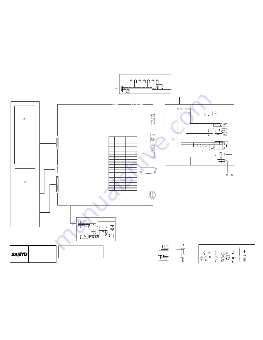
A101A

1

AGC

2

3

AS

4

SCL

5

SDA

6

MB

7

MB

8

9

TU

10

11

IF

12

13

14

15

K7J

1

2

3

4

5

1

2

3

4

5

6

7

KC

1

1

2

3

3

KX

1

2

3

4

5

KA

1

2

3

4

5

KF

1

1

2

3

4

4

1

1

2

3

4

5

6

7

8

9

10

11

12

13

14

14

1

1

2

2

3

4

5

6

7

8

9

10

11

12

13

14

15

16

17

18

19

19

20

20

K1004

AV2

1

2

3

4

5

6

7

8

9

R

W

Y

V_IN

R_IN

L_IN

1

HEAD-PHONE

3

5

7

AR3_IN

2

6

4

AL3_IN

ASSY,PWB,SIDE-AV,N2SV

1AA0B10N135BA

+OUTR

+OUTL

V3_IN

1/16

GZ0C

R2402

1/16

GJ100KC

R2407

L2C4

100KJ

L2402

K29X_1

1/16GJ

100KC

R2401

1/16

GJ2.2KC

R2406

GND1

CJ100

CGQ

C2403

K29X_3

X

C2402

CJ100

CGQ

C2406

1/16

GJ100KC

R2404

X

C2401

CJ100

CGQ

C2407

L2C4

100KJ

L2403

K29X_5

CJ100

CGQ

C2404

1/16

GJ2.2KC

R2403

R

W

Y

J12B4080N

K2401

1

2

3

5

6

4

K29X_G

GND1

K2402_2

KSP24L_1

R2414

1/2GJ150

J12B06000

K2402

X

C2424

K29F_4

L26B2770G

L2404

KSP24R_1

K2402_5

KZ0.01

GQF

C2416

KZ0.01

GQF

C2413

KZ0.01

GQF

C2415

K2402_4

X

C2421

16PM10DK

C2418

K2402_6

KZ0.01

GQF

C2414

X

C2419

KSP24L_2

KSP24R_3

K2402_1

K29F_1

K2402_3

L26B2770G

L2405

L26B2770G

L2406

R2415

1/2GJ150

X

C2423

16PM10DK

C2417

X

C2420

K2402_7

X

C2422

K29F_G

X

R2416

X

R2417

J10AV043N

K29F

1

1

2

3

4

4

J10AV053N

K29X

1

2

3

4

5

J10AV023N

KSP24L

1

1

2

2

J10AV033N

KSP24R

1

3

X

SC2401

1

2

X

SC2402

1

2

X

SC2403

1

2

X

SC2404

1

2

X

SC2405

1

2

SH1

1

SH2

1

CJ1000

CGQ

C2425

GND1

GND1

TO KC

POS+

VOL-

POWER_SW

POS-

VOL+

1AA0B10N135BB

ASSY,PWB,KEY,N2SV

OK

MENU

KEY_IN

POWER_KEY

1/16

GJ10C

R2957

1/16

GJ100C

R2951

K29C_G

1/16

GJ270C

R2955

S10B3530G

SW2957

1

2

3

4

1/16

GJ560C

R2953

S10B3530G

SW2956

1

2

3

4

S10B3530G

SW2954

1

2

3

4

S10B3530G

SW2953

1

2

3

4

S10B3530G

SW2955

1

2

3

4

1/16

GJ1KC

R2952

K29C_1

S10B3530G

SW2951

1

2

3

4

K29C_2

X

SC2952

1

2

1/16

GJ220C

R2956

S10B3530G

SW2952

1

2

3

4

1/16

GJ390C

R2954

J10EG035G

K29C

1

1

2

3

3

X

SC2951

1

2

UDZS10BG

D2951

UDZS10BG

D2952

TO KA

RC

LED

1AA0B10N135BC

ASSY,PWB,LED,N2SV

KK1000GQ

C2904

K29A_G

K29A_3

1/16

GJ100C

R2901

K29A_2

X

SC2902

1

2

1/16GJ390C

R2905

K29A_1

1/16GJ100C

R2902

5VCPU

SLP-181B51

D2901

VCC

VOUT

GND

GND

GND

U20B24401

A2901

1

2

3

4

5

SCREW_14

S2901B

1

2

3

4

5

6

7

8

9 10 11 12 13 14

SCREW_14

S2902B

1

2

3

4

5

6

7

8

9 10 11 12 13 14

J10AV053N

K29A

1

2

3

4

5

6.3KK10MB

C2902

:6.3KM10GMB

5VCPU

X

R2906

X

Q2901

X

C2905

X

R2907

X

D2903

X

D2902

UDZS

10BG

D2904

J30B1640G

TP2901

:J30A00102

J30B1640G

TP2902

:J30A00102

Z30B0220G

SC2903

1

2

Z30B

0220G

SC2904

1

2

X

SC2905

1

2

X

SC2906

1

2

6.3KK10MB

C2901

:6.3KM10GMB

X

SC2907

1

2

17/23inch

17inch

23inch

EL901

LCD MODULE

Model LCD-23XL2: 

1AV4T40B60001

 or

1AV4T40B60002

Model LCD-17XL2:

1AV4T40B60102

INVERTER UNIT

Model LCD-17XL2:

1AV4U20B81300

Model LCD-23XL2: 

Included in LCD Module

J10AU070N

K7K

K7L

K7H

DC INPUT

TERMINAL

SIGNAL UNIT

DIFFERENCE LIST 

1AA0B10N150DA

ASSY,PWB,SIGNAL,N2SV

Model LCD-17XL2:

1AA0B10N150EA

ASSY,PWB,SIGNAL,N2RV

Model LCD-23XL2:

ASSY,PWB,SIGNAL

K1002AV1

K1005

AV2

1/16GJ10KC

1/16GF1KC

1/8GZ000

1/16GJ6.8KC

1/8GZ000

R6639

X

X

1/16GJ10KC

R704

R6602

C010

X

R6643

X

X

1/16GF10KC

1/16GZ0C

R1606

X

R6605

R4043

X

K7L

10KK2.2GQ

X

1/16GJ33KC

1/8GZ000

X

1AA0B10N150DA

1/16GJ3.9KC

R6606

1/16GF15KC

1GJ150

1/16GJ10KC

1GJ180

R705

1/8GZ000

25EM4704U

1/16GZ0C

1/16GZ0C

X

1/16GZ0C

Model LCD-23XLP

R6603

1/16GJ12KC

1/8GZ000

J10AU065N

C6605

1GJ560

1/16GZ0C

1GJ560

R001

R6629

1GJ560

25EM10004U

1/16GJ3.9KC

1/10GZ0.0

1/16GF560C

R6607

1/8GZ000

X

R6669

R6600

X

1/8GZ000

R706

JS1601

25EM4704U

1AA0B10N150EA

X

X

1/16GJ15KC

R6638

X

R6644

R6630

R6604

C009

X

1/16GJ8.2KC

X

R002

X

X

1GJ560

R6612

1/8GZ000

X

R708

25EM10004U

R6601

J10AV143N

25KZ0.1GQF

R4042

K7K

Model LCD-17XLP

1

2

1

2

SP1101

SP1102

COLOUR TELEVISION

CHASSIS
SERIES

SERVICE 
REF. NO.

U

U

U

U

E

E

E

E

1

1

1

1

--

--

B

B

B

B

PRODUCT SAFETY NOTICE:

Product safety should be considered when a component replacement is made  in any
area of a receiver.

Components indicated by a mark 

in this circuit diagram show components whose

values have special significance to product safety. It is particularly recommended that
only parts specified on the part service manual be used for components replacement
pointed out by the mark.

CIRCUIT DIAGRAM NOTICE:
1. All resistance value are in ohms, K=1,000, M=1,000,000.
2. All resistance rated wattages are 1/6W unless otherwise noted.
3. Excepting electrolytic capacitors, all capacitance values of less than 1are expressed in µ F 

and more than 1 are µF.

4. All capacitance rated voltages are 50V unless otherwise noted.
5. All inductance values are in µ H.
6. This circuit diagram covers a basic or representative chassis only. There may be some 

components or partial circuit differences between the actual chassis and the circuit diagram.

7. Parts specified with "X" are not installed in this model.
8. Parts specified with "J" are just jumper wires.

9. Expression of capacitance and resistance in circuit diagrme.

N2SV/N2RV

TRANSISTOR, DIODE AND INTEGRATED CIRCUIT TERMINAL GUIDE

C: COLLECTOR
B: BASE
E: EMITTER

A: ANODE
K: KATHODE

B

B

C

C

E

E

C E

B

C E

B

B

C

E

A

K

K

A

A

K

FUSIBLE
RESISTOR

PARTICULAR

PARTS SYMBOL

1

1

1

N/2

N/2 + 1

N

NON POLE
ELECTRIC
CAPACITOR

POSISTER

C

E

B

CHIP 
COMPONENTS

K

A

TRANSISTOR

DIODE

123

RESISTOR

12 X 103=12K

Capacitance (Example)

1000  C M 2000 D

Characteristic
Capacitance value (220pF)
Allowable error (

±

20%)

Kind (Ceramic)
Rated voltage (1,000V)

J= 

±

 5%

K= 

±

10% 

M= 

±

20%

Resistance (Example)

1/2  N J 1.2

Resistance value (1.2

)

Allowable error (

±

5%)

Kind (M.carbon)
Rated wattage (1/2W)

D: Carbon
N: Metalized carbon
S: Oxied metalized
W: Wire wounding
C: Solid

T, A, U, D: 

Electrolytic

C, K, B: Ceramic
F: Mylar film
M, N: Polypropylene
Z: Metalized paper

LCD-17XL2-00
LCD-23XL2-00

Содержание LCD-23XL2

Страница 1: ...n system and power source differ from the design specifications Refer to the specification table Product Code 111374316 Original Version Chassis Series UE1 B Service Ref No LCD 23XL2 00 Contents Safety Notice 2 Specifications 3 Chassis Block Diagrams 4 5 CPU Port Functions 6 Option Setting 7 On screen Service Menu System 8 10 Service Adjustments 11 Protection Circuit 12 Mechanical Disassembly 13 1...

Страница 2: ...ay parts or tools have been left inside Before returning any television to the customer the service personnel must be sure that it is completely safe to operate without danger of electrical shock Product Safety Notice Product safety should be considered when a component replacement is made in any area of a receiver Components indicated by mark in the parts list and the schematic diagram designate ...

Страница 3: ... 1280 Horiz x 720 Vert pixels Viewing Angles Horiz 176 Vert 176 Contrast Ratio 800 1 Brightness 550 cd m2 Audio Output RMS 5W 5W Speaker 5 cm x 9 cm x 2 pcs AV Input Terminals AV1 Video Composite Video Input x 1 AV1 Audio L R Stereo Input x 1 set AV2 or DVD Video Composite Component Y CB CR Input x 1 set AV2 S Video Separated Y C DIN Jack Input x 1 AV2 Audio L R Stereo Input x 1 set AV3 Video Comp...

Страница 4: ... K7H LVDS0N LVDS0P LVDS1N LVDS1P LVDS2N LVDS2P LVDS_CLKN LVDS_CLKP LVDS3N LVDS3P V COMPISITE VIDEO IN AV3 B21 AV3 D2901 LED A2901 RC RECEIVER TOP CONTROL KEYS SW2951 SW2957 RC IN ASSY PWB LED ASSY PWB SIGNAL KX K29X K29A ASSY PWB KEY KA K29C KC AA25 AE20 STAND BY POWER INDICATOR AE25 AE22 POWER KEY IN KEY IN COMPISITE VIDEO IN B19 V23 V24 U23 D18 C18 S VIDEO C IN S TERMINAL AV2 S VIDEO Y IN COMPON...

Страница 5: ...WB KEY KA K29C KC AA25 AE20 STAND BY POWER INDICATOR AE25 AE22 POWER KEY IN KEY IN IC001 AUDIO AMP C17 D17 AUDIO L AUDIO R 4 2 8 12 SP902 SP901 K001 HEADPHONE JACK AUDIO R OUT AUDIO L OUT R OUT L OUT KF K29F ASSY PWB SIDE AV L B20 EXT AUDIO R IN AV3 EXT AUDIO L IN AV3 R IN L IN IC201 IF VIDEO CHROMA CPU SCALER CAPTION AUDIO CONTROL F24 EXT AUDIO IN R AV1 A23 C21 EXT AUDIO IN L AV1 EXT AUDIO IN R A...

Страница 6: ... RC input INT0 P0 5 External interrupt 0 or port 0 5 320 AC18 Status input P0 2 I2SDO2 Port 0 2 or I2S digital output 2 319 AC19 I2C SDA P1 7 SDA Port 1 7 or I2C bus data line 241 AD18 Power Error 2 P0 3 I2SCLK Port 0 3 or I2S clock Power Error Low 240 AD19 I2C SCL P1 6 SCL Port 1 6 or I2C clock line 239 AD20 RGB selector P2 2 PWM1 Port 2 2 or PWM1 output 238 AD21 Scart 2 8 pin input P3 1 ADC1 Por...

Страница 7: ...tion items and default setting mode Option Items Mode Default Description OSD H POS 0 to 15 Default 6 OSD horizontal position adjustment COUNTRY ARG BRA or Default ARG Argentina Shipping country selection SOUTH AMERICA PLUG PLAY ON or OFF Default ON Disable or enable Plug Play function SURROUND ON or OFF Default ON Disable or enable Surround function Incase of inactive the Sound menu will have no ...

Страница 8: ...ta The or key will increase or decrease the data sequentially On screen Service Menu System 1 How to enter the Service Menu Press and hold the SOUND MODE button of the remote control and press the CHANNEL DOWN P button on the top control panel of the TV Item No Adjustment Item Adjustment Data P 17 0 1 1 1 0 0 0 0 0 0 0 0 0 0 0 0 0 1 1 1 0 0 0 0 0 0 1 0 1 1 0 1 1 0 0 0 0 1 0 1 0 0 1 0 1 1 0 1 0 0 0...

Страница 9: ...ckstretch Black stretch 1 076 Bluestretch Blue stretch 0 077 Whitestretch Gamma control and white stretch setting 0 078 GAM Gamma control 0 079 PWL Peak White limiting 0 No Title Explanation Initial Value 080 BSD Black stretch Depth 0 081 AAS Black stretch Area Selection 0 082 PeakRatioOvShot Ratio of positive and negative peak 0 083 RatioPreAftShot Ratio pre and after shoot 0 084 CRAO Coring on S...

Страница 10: ...8 SVO Function of IFVO SVO CVBS1 pin 0 199 GD Group delay on CVBS1 signal 1 200 BPB Bypass of sound bandpass filter at mono mode 0 201 BPB2 Bypass of sound bandpass filter section 2 1 202 OSD H POS On screen Display Horizontal position 6 203 CL Cathode drive level 0 204 PGR Preset Gain Red 45 205 PGG Preset Gain Green 45 206 PGB Preset Gain Blue 45 207 Back Light Back light 63 208 BL PWMMin Back l...

Страница 11: ...ns Screen Size FULL Picture Mode DYNAMIC White Balance Adjustment 1 Enter the Service Mode Adjustment Item No 147 SAGR ADC Gain Red No 148 SAGG ADC Gain Green No 149 SAGB ADC Gain Blue 2 Decide a fixed item which is maximum value 31 Example let 31 of No 147 SAGR be maximum value select item of other 2 colours Example No 148 SAGG or No 149 SAGB with or key and adjust to produce a normal black and w...

Страница 12: ...e circuit will have to be repaired When operating the Protection Circuit the Stand by and Power Indicator will blink The number of blinks will be determined by the type of failure detected as shown below 1 One time blinks Power failure of Video Decoder in IC 201 2 Two times blinks Scaler error of IC 201 3 Three times blinks Power failure of 2 5 V DecDig supply in IC 201 In case of 2 5V falls less ...

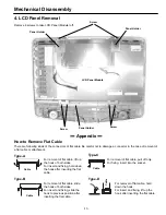
Страница 13: ...tion TV face down on a padded or cushioned surface to protect the screen and finish 2 Remove one screw and remove a stand cover 3 Remove 3 screws to take the stand off CAUTION Hold the stand firmly as you remove the last screw Stand Cover Screw Screws ...

Страница 14: ...14 Mechanical Disassembly 2 Cabinet Back Removal 1 Remove side cover 2 Remove 13 screws and take the Cabinet Back off Note Cabinet Back can be removed even if it does not remove a stand Remove side cover ...

Страница 15: ...net Back and Stand remove Top Cover Side Frame and Cabinet Bottom Location of Circuit Board and Electrical Parts ASSY PWB KEY ASSY PWB SIDE AV Speaker Speaker INVERTER UNIT Chassis Frame ASSY PWB LED Cabinet Bottom Top Cover Side Frame LCD Panel Module ASSY PWB SIGNAL ...

Страница 16: ... chassis can be taken out Chassis Frame ASSY PWB KEY ASSY PWB SIDE AV ASSY PWB LED Remove 2 screws to take the chassis out LCD Panel Module ASSY PWB SIGNAL For Gasket The gasket is provided to prevent exposure of interference for other radio and television receptions The gasket should be replaced on previous positions after servicing ...

Страница 17: ...ble or attachment Type A For removal of flat cable lift up the hook of both sides For insert and fixing hold down the hook after inserting the flat cable Cable Type B For removal of flat cable slide the hook of both sides For insert and fixing slide the hook to previous position after inserting the flat cable Cable Type C Cable For removal of flat cable pull off only For fixing insert into the soc...

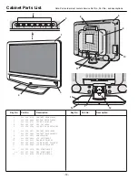
Страница 18: ...0 325 6726 COVER USB SHEET N2RV 6 610 324 8622 CABINET BACK N2RV 7 610 324 8943 CABINET BOTTOM N2RV 8 610 321 1831 HANDLE N2RJ 9 610 324 8844 LID SIDE N2RV 10 610 324 9001 FRAME SIDE N2RV 11 610 324 8813 COVER SHAFT TOP N2RV 12 610 324 8882 COVER SHAFT N2RV 13 610 322 3278 DEC STAND N2RC or 610 322 5289 DEC STAND N2RY 14 610 321 8328 STAND TOP N2RC Key No Part No Description Key No Part No Descrip...

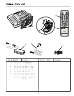
Страница 19: ...5 072 9782 ASSY REMOCON JXMTF 17 610 297 9879 RC BATTERY LID JXMTA 18 645 081 2705 CORD POWER 2 0MK ARG 19 645 075 9666 ADAPTOR AC DC 20 645 082 5941 PLUG ADAPTOR ANT PAL or 652 001 7528 PLUG ADAPTOR ANT PAL 610 324 8004 INSTRUCTION MANUAL N2RV Spanish Key No Part No Description Key No Part No Description 15 ...

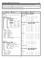
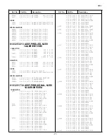
Страница 20: ...s List Ref No Part No Description Ref No Part No Description Product safety should be considered when a component replacement is made in any area of a receiver Components indicated by a mark in this parts list and the circuit diagram show components whose value have special significance to product safety It is particularly recommended that only parts specified on the following parts list be used f...

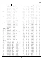
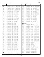
Страница 21: ... L6 TB 405 015 8922 TR 2SC2812 L7 TB 405 163 1612 TR 2SC2812N L6 TB0 405 173 9813 TR 2SC3928A1R 405 173 9912 TR 2SC3928A1S Q202 405 212 1617 TR 2SA2048 Q TSMT3 405 171 8511 TR 50A02CH TL E Q203 405 212 1617 TR 2SA2048 Q TSMT3 405 171 8511 TR 50A02CH TL E Q204 405 014 4519 TR 2SC2412K T146 R 405 014 4618 TR 2SC2412K T146 S 405 015 8724 TR 2SC2812 L6 TB 405 015 8922 TR 2SC2812 L7 TB 405 163 1612 TR ...

Страница 22: ...P J 50V C102 403 215 2211 CERAMIC 0 01U K 50V C1021 403 157 3611 CERAMIC 100P J 50V C1022 403 157 3611 CERAMIC 100P J 50V C1023 403 157 3611 CERAMIC 100P J 50V C1024 403 157 3611 CERAMIC 100P J 50V C1025 403 157 3611 CERAMIC 100P J 50V C103 403 398 1513 ELECT 1000U M 6 3V C104 403 215 2211 CERAMIC 0 01U K 50V C1043 403 207 0317 CERAMIC 1U Z 16V C1044 403 207 0317 CERAMIC 1U Z 16V C1045 403 207 031...

Страница 23: ... 0214 CERAMIC 0 1U Z 25V C4029 403 113 3815 CERAMIC 1000P K 50V C4031 403 164 0214 CERAMIC 0 1U Z 25V C4032 403 164 0214 CERAMIC 0 1U Z 25V C4033 403 164 0214 CERAMIC 0 1U Z 25V C4034 403 372 7517 CERAMIC 2 2U K 6 3V C4036 403 113 3815 CERAMIC 1000P K 50V C4037 403 164 0214 CERAMIC 0 1U Z 25V C4038 403 368 7316 CERAMIC 10U K 6 3V 403 370 7618 CERAMIC 10U M 6 3V C4039 403 368 7316 CERAMIC 10U K 6 3...

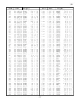
Страница 24: ...243 401 105 1115 MT GLAZE 12K JA 1 16W R1244 401 105 1115 MT GLAZE 12K JA 1 16W R1246 401 105 0415 MT GLAZE 100 JA 1 16W R1247 401 105 0415 MT GLAZE 100 JA 1 16W R1248 401 105 0613 MT GLAZE 10K JA 1 16W R1249 401 105 0613 MT GLAZE 10K JA 1 16W R132 401 105 0613 MT GLAZE 10K JA 1 16W R141 401 037 5014 MT GLAZE 0 000 ZA 1 10W R142 401 037 5014 MT GLAZE 0 000 ZA 1 10W R143 401 037 5014 MT GLAZE 0 000...

Страница 25: ...JA 1 16W R6628 401 105 4215 MT GLAZE 33K JA 1 16W R6629 401 212 0018 MT GLAZE 15K FA 1 16W R6630 401 230 2513 MT GLAZE 1K FA 1 16W R6631 401 218 4416 MT GLAZE 1 2K FA 1 16W R6638 401 230 4616 MT GLAZE 560 JA 1W R6639 401 230 4616 MT GLAZE 560 JA 1W R6640 401 105 0712 MT GLAZE 100K JA 1 16W R6641 401 105 4215 MT GLAZE 33K JA 1 16W R6642 401 105 4215 MT GLAZE 33K JA 1 16W R6643 401 230 4616 MT GLAZE...

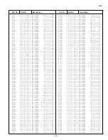
Страница 26: ...07 206 5618 ZENER DIODE UDZS TE 1710B D1005 407 206 5618 ZENER DIODE UDZS TE 1710B D1009 407 206 5618 ZENER DIODE UDZS TE 1710B D101 407 149 0817 DIODE 1SS355 TE 17 D102 407 149 0817 DIODE 1SS355 TE 17 D1020 407 206 5618 ZENER DIODE UDZS TE 1710B D1021 407 206 5618 ZENER DIODE UDZS TE 1710B D1022 407 206 5618 ZENER DIODE UDZS TE 1710B D103 407 149 0817 DIODE 1SS355 TE 17 D104 407 228 4910 ZENER DI...

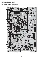
Страница 27: ...3 D1003 C6618 8 5 1 4 Q1600 Q1601 R1001 C1606 D1006 R1002 C1607 D1007 D1008 C1221 C1222 1 3 KC C1223 R1007 C1224 C6620 D1201 D1202 C1226 R126 C6622 C1227 C6624 D6600 R129 R1201 C6625 D6601 R1202 8 1 KJ C1612 D1012 R1203 C1613 D1013 R1204 C6628 D860 C1038 C1614 D1014 R1205 C6629 C1039 R1206 R1207 D6607 R1208 R6604 R130 D6608 R6605 C1231 D1019 D6609 R132 C1233 C6630 C1234 R710 IC6600 C1040 R135 R711...

Страница 28: ... R108 Q6600 R109 C6605 Q6604 C1018 C6609 Q6605 C1019 Q6606 Q6607 Q6608 R110 R111 C1020 C1021 C1022 C1023 C1024 D1001 D1002 C6617 D1004 D1005 R1003 R1004 D1009 R122 R1006 R125 C6621 R1009 R702 D1203 R127 R703 R128 R704 R705 R706 C6627 R707 R6600 R708 R6601 R1011 R709 R6602 R1012 R6603 D1017 R1013 D1018 R1014 SC101 SC102 R6606 R6607 R1017 R6608 C6631 R6609 JS801 C6632 C1043 C6634 D1020 C1044 D1021 C...

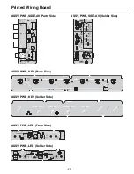
Страница 29: ... SC2403 SC2404 SC2405 ASSY PWB KEY Solder Side ASSY PWB KEY Parts Side B10N1240B PWB KEY N2RJ POW_SW POS POS VOL VOL OK MENU SW2951 SW2952 SW2953 SW2954 SW2955 SW2956 SW2957 D2951 D2952 R2951 R2952 R2953 R2954 R2955 R2956 R2957 SC2951 SC2952 K29C 3 1 ASSY PWB LED Solder Side ASSY PWB LED Parts Side B10N1240C PWB LED N2RJ D2901 D2902 A2901 K29A 1 5 R2901 R2905 R2906 TP2901 TP2902 D2904 SC2905 C2901...

Страница 30: ...Oct 05 NEWSAN S A Una empresa del grupo SANYO Electric Co ...

Страница 31: ...AL SIGNAL UNIT DIFFERENCE LIST 1AA0B10N150DA ASSY PWB SIGNAL N2SV Model LCD 17XL2 1AA0B10N150EA ASSY PWB SIGNAL N2RV Model LCD 23XL2 ASSY PWB SIGNAL K1002AV1 K1005 AV2 1 16GJ10KC 1 16GF1KC 1 8GZ000 1 16GJ6 8KC 1 8GZ000 R6639 X X 1 16GJ10KC R704 R6602 C010 X R6643 X X 1 16GF10KC 1 16GZ0C R1606 X R6605 R4043 X K7L 10KK2 2GQ X 1 16GJ33KC 1 8GZ000 X 1AA0B10N150DA 1 16GJ3 9KC R6606 1 16GF15KC 1GJ150 1 ...

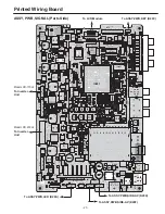
Страница 32: ...1 SC2_G L2GL391JG L102 TUNGND 16KK0 47BA C1233 K7K 1 2 3 4 5 6 K7I_5 CJ220CGQ C4063 5V_SW X TP6609 KC_1 25KZ0 1GQF C264 TUNGND LVDS3P L3BQ102PG L214 TV_VS 1 16GZ0C JS1206 R1A44704G RB4007 R1EA4704G SCL 6 3KK10MB C206 6 3KM10GMB X Q6605 L3CG601PG L700 1 2 3 4 5V_SW 25KZ 0 1GQF C4006 KK 4700GQ C113 K7L_12 1SS355 D1202 B4J11B0210N K7J 1 2 3 4 5 25KZ 0 1GQF C6627 X C702 X KP2B 1 2 3 4 5 KK 0 01GQ C122...

Отзывы: