


No. 5995-8/34
LC78626KE
Description of Pins
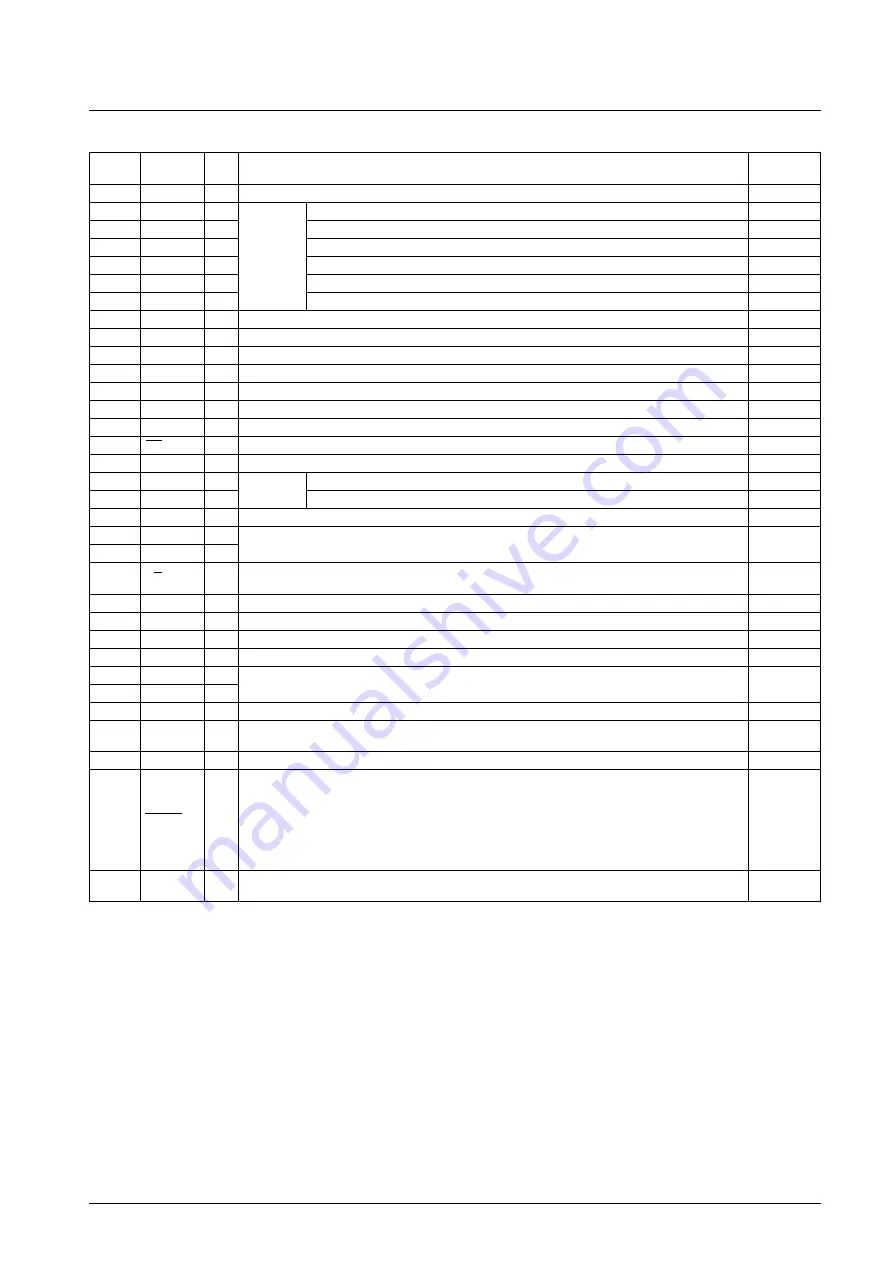
Pin
Pin
I/O
Function
Output pin states
No.
Name
during reset
1
DEFI
I
Defect detection signal (DEF) input. When not used, must be connected to 0 V.
—
2
TAI
I
Test input. Equipped with internal pull-down resistor. Must be connected to 0V.
—
3
PDO
O
Internal VCO control phase comparator output
—
4
VV
SS
P
For the PLL
Internal VCO ground. Must be connected to 0 V.
—
5
ISET
AI
PDO output current adjustment resistor connection
—
6
VV
DD
P
Internal VCO power supply
—
7
FR
AI
VCO frequency range adjustment
—
8
V
SS
P
Digital system ground. Must be connected to 0 V.
—
9
TESCLK
I
Test clock input. Must be connected to V
DD
.
—
10
TESA
I
Test operation mode control input. Must be connected to V
DD
.
—
11
TESB
I
Test operation mode control input. Must be connected to V
DD
.
—
12
TESC
I
Test operation mode control input. Must be connected to V
DD
.
—
13
TESGB
I
Test operation mode control input. Must be connected to V
DD
.
—
14
TEST5
I
Test input. Equipped with internal pull-down resistor. Must be connected to 0 V.
—
15
CS
I
Chip select input. Equipped with internal pull-down resistor. When not controlled, must be connected to 0 V.
—
16
TEST1
I
Test input. Must be connected to 0 V.
—
17
EFMO
O
For slice
EFM signal output
Undefined
18
EFMI
I
level control
EFM signal input
—
19
TEST2
I
Test input. Equipped with internal pull-down resistor. Must be connected to 0 V.
—
20
CLV
+
O
Disk motor control output. Can have a 3-state output depending on the command.
Low-level output
21
CLV
–
O
22
V/P
O
Low-level output
23
HFL
I
Track detect signal input. Schmidt input.
—
24
TES
I
Tracking error signal input. Schmidt input.
—
25
TOFF
O
Tracking off output
High-level output
26
TGL
O
Tracking gain switch output. Gain is increased with low level.
Undefined
27
JP
+
O
Track jump control output. Can be 3-state output depending on the command.
Low-level output
28
JP
–
O
29
PCK
O
EFM data playback clock monitor. 4.3218 MHz during phase lock.
Low-level output
30
FSEQ
O
Undefined
31
V
DD
P
Digital system power supply
—
32
ASRES
I(I/O)
Input mode
33
CONT2
I/O
Input mode
Continued on next page.
Rough servo/phase control automatic switching monitor output. If a high level then rough servo mode.
If a low level then phase control mode.
Sync signal detect output. A high level when the sync signal detected from the EFM signal matches the
internally generated sync signal.
Reset signal input for initializing only the anti-shock control part (i.e. excluding the DSP part). Resets when
this pin is low level, and release the reset when this pin is high level. Tie this pin to the low level (i.e.,
connected to 0 V) if when using software control on the anti-shock part alone through the anti-shock part
only reset disable/release command ($F4) or the anti-shock only reset enable/inrush command ($F5).
Note: This pin is assigned as the least significant bit of the general I/O port however, use as a general I/O
pin is disabled. When the port I/O set command ($DB) is executed, the least significant bit is always “0,” and
the output driver is not turned ON.
General I/O pin 2. This controls the commands from the microcontroller. When not used, either set this as
an input port and connect to 0 V, or set this as an output port and leave it open.


