


-10-
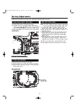
Service Adjustments with Replacing Memory IC(IC801)
(/JE0291A)
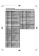
DATA
INITIAL
No.
ITEM
RANGE SETUP
DESCRIPTION
DATA
01
RFAGC
0~63
27
RF AGC Adj.
02
H-PHA
0~31
13
H-Phase (H-Centering) Adj. (50Hz)
03
V-POS
0~63
40
V-Position Adj.(50Hz)
04
V-SHIFT
0~15
5
V-Phase (V-Centering) Adj. (50Hz)Fixed.
05
V-SIZ
0~127
40
V-Size Adj. (50Hz)
06
V-LIN
0~31
20
V-Linearity Adj. (50Hz)
07
V-SCO
0~31
8
V-S-Correction (50Hz)
08
VTRANS
0, 1
0
Data transmission between V Retrace
09
VRES
0, 1
0
Vertical Reset Timing
10
H-P60
-16~+15
+3
H-Phase Adj. (60Hz) difference val.
11
V-S60
-64~+63
-10
V-Size Adj. (60Hz) difference val.
12
V-SHIF60
-16~+15
-4
V-Phase Adj. (60Hz) difference val.
13
OSDHP
0~255
31
OSD H-Position Adj.
14
OSDC
0~3
4
OSD Contrast Adj.
15
V-SCP
0~7
7
V-Size COMP Adj.
16
SBIAS
0~255
105
Sub Bias Adj.
17
RBIAS
0~255
0
Red Bias Adj.
18
GBIAS
0~255
0
Green Bias Adj.
19
BBIAS
0~255
0
Blue Bias Adj.
20
RDRIV
0~127
64
Red Drive Adj.
21 GDRIV
0~15
8
Green Drive Adj.
22
BDRIV
0~127
64
Blue Drive Adj.
23
1 Line Appear
White Balance Adj.
24
DRV
White Balance Adj.
25
B-YD
0~15
10
B-Y DC Level Adj.
26
R-YD
0~15
9
R-Y DC Level Adj.
27
B-YDN
-16~+15
0
NTSC B-Y DC level Adj.
28
R-YDN
-16~+15
0
NTSC R-Y DC level Adj.
29
SBDC
-16~+15
0
SECAM B-Y DC Level Adj.
30
SRDC
-16~+15
0
SECAM R-Y DC Level Adj.
31
B-YDD
-16~+15
0
DVD B-Y DC Level Adj.
32
R-YDD
-16~+15
0
DVD R-Y DC Level Adj.
33
RGBTEMP
0, 1
0
RGB Temp SW
34
RGBTEST
0, 1
0
RGB Test
35
DRVTEST
0, 1
0
Drive Test Mode
36
HALFTONE
0, 1
2
Halftone Color
37
G-YA
0, 1
0
G-Y Angle
38
GYAMP
0~15
8
G-Y Amplitude Adjust
39
RBGB
0~15
8
R-Y / B-Y Gain Balance
40
RBAG
0~15
8
R-Y / B-Y angle
41
G-YAN
0, 1
0
NTSC G-Y Angle
42
GYAMPN
-8~+7
0
NTSC G-Y Amplitude Adjust
43
RBGBN -16~+15
0
NTSC R-Y / B-Y Gain Balance
44
RBAGN -16~+15
0
NTSC R-Y / B-Y Angle
45
RBGBDN
-16~+15
+10
DVD NTSC R-Y / B-Y Gain Balance
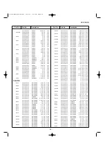
Following table shows the initial values which have been stored in the CPU ROM, and items for the service adjustments.
Service mode adjustments table in CPU ROM
DATA
INITIAL
No.
ITEM
RANGE SETUP
DESCRIPTION
DATA
46
RBAGDN
-16~+15
+10
DVD NTSC R-Y / B-Y Angle
47
VOLFIL
0, 1
0
DAC Volume filter disable
48
IF-AGC
0, 1
0
IF AGC defeat
49
COGV
0~3
0
Coring Gain
50
BLKS
0~3
3
Blk.str.start(W/Defeat)
51
BLKG
0~3
3
Blk.str.gain
52
BRTA
0, 1
0
Brt.Abl.Def
53
BRST
0, 1
0
Mid.Stp.Def
54
BRTH
0~7
0
Bright.Abl.Treshold
55
WPL
0~3
2
White Peak Limit Op. Point (w/ defeat)
56
YGAM 0~3
0
Y Gamma
Start
57
PRS
0~3
0
Pre-shoot AV Adj.
58
ORS
0~3
0
Over-shoot AV Adj.
59
DCREST
0~3
0
Select Luminance DC Restoration
60
RFCO
0~3
2
RF Coring Gain Difference
61
PRSN
0~3
0
Pre-shoot RF Adj.
62
ORSN
0~3
0
Over-shoot RF Adj.
63
CTRAP
0~7
4
Chroma Trap Control
64
CBPF
0~3
1
Chroma BPF Control
65
CBPFN
0~3
1
Chroma BPF Control NTSC
66
CBPFAVN
0~3
0
Chroma BPF Control AV NTSC
67
TINT
-16~+15
+10
Tint RF
68
TINT443 -16~+15
-12
Tint (NTCS4.43)
69
SHRF
-32~+31
-10
RF Sharpness
70
COLTEST
0, 1
1
Color Test
71
CODP
-16~+15
0
DVD PAL Color
72
CODN
-16~+15
0
DVD NTSC Color
73
TINTDN -16~+15
0
Color Killer Option
74
YTH
0~3
0
Select Y signal sensitivity for Blue Strect
75
YGAIN
0~3
0
Select Blue Stretching gain w/ defeat
76
RWIDTH
0~3
0
R Width
77
ROFFSET
0~3
0
R Offset
78
BWIDTH
0~3
0
B Width
79
BOFFSET
0~3
0
B Offset
80
VOLUM
0~127
127
Volume Control Adj.
81
DEEM
0, 1
0
De-emphasis TC
82
VIFSW
0~3
0
VIF System Switch
83
SIFSW
0~3
1
SIF System Switch
84
V-LVL
0~7
4
Video Level
85
V-LVLOFS
0~3
1
Video Level Offset
86
FMGAIN
0, 1
0
FM Gain
87
IFOM-S
0, 1
0
Over Modulation Switch
88
IFMN-S
0, 1
1
Audio Monitor Sw. Monitor or FM
89
IFTRPS
0, 1
1
IC inside SIF Trap Sw ON-OFF
90
IFMLVL
0~15
0
IF Over Modulation Level Adj.
SM_14-BB3V;W(AC6-A1)Aus,NZ 10/9/06 2:25 PM Page 10


