Schematic Diagrams
Samsung Electronics
This Document can not be used without Samsung's authorization
7-
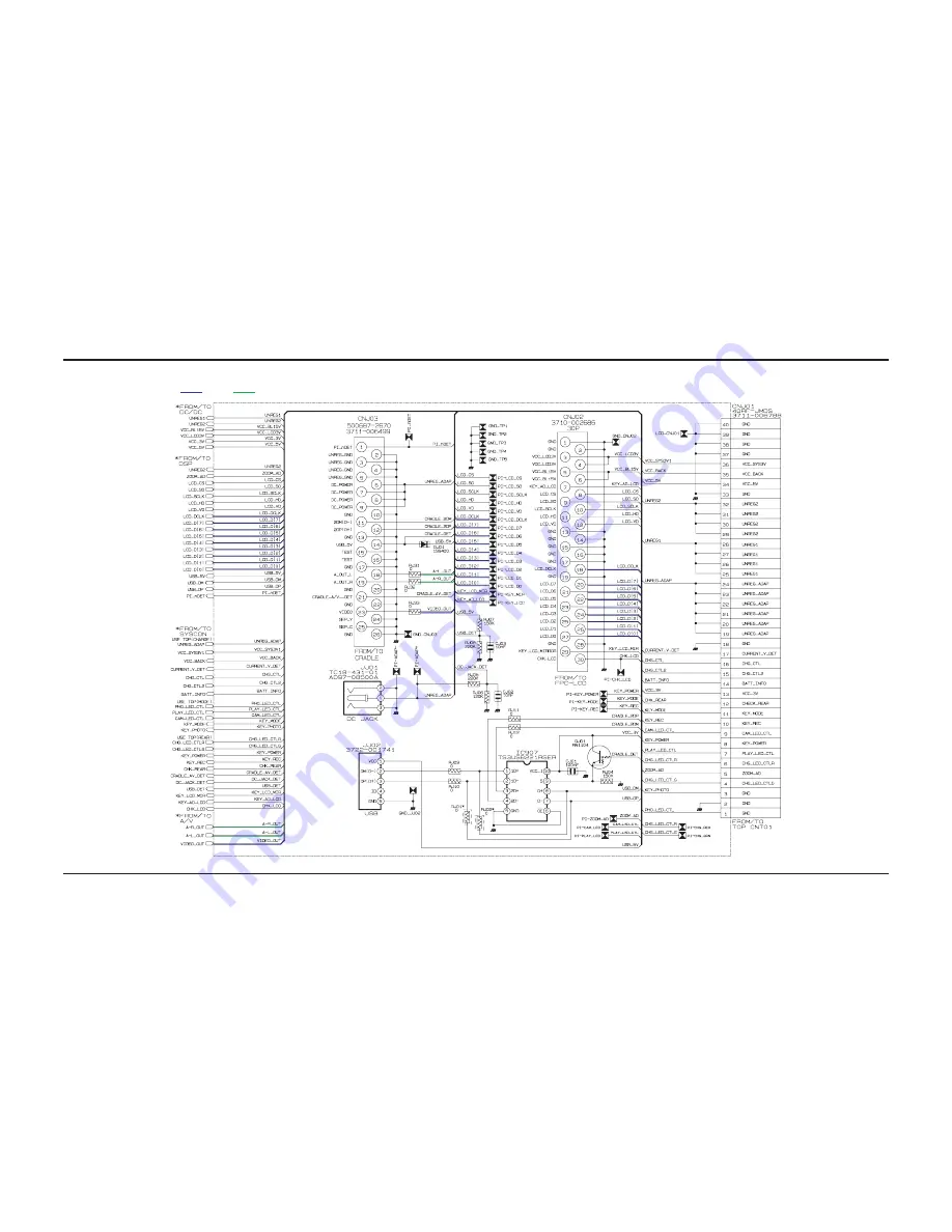
7-11 Jack (Main PCB)
VIDEO
AUDIO
Страница 1: ...MX20 Application Models VP MX20 VP MX20H VP MX20P VP MX20R VP MX20C VP MX20CH VP MX20CN VP MX20L Application Area XEF XEU XEG XET XEV XEC XSA CDM XST XEO XEH XEP XEE EAP EUR XEN HACO TAW TIT COL SEO X...
Страница 2: ...12 6 PCB Diagrams 6 1 6 10 6 1 Wiring Diagram 6 2 6 2 Main PCB 6 3 6 3 LCD PCB 6 5 6 4 Rear PCB 6 6 6 5 CCD PCB 6 7 6 6 Top PCB 6 8 6 7 LCD FPC 6 9 6 8 Mode FPC 6 9 7 Schematic Diagrams 7 1 7 20 7 1...
Страница 3: ...a metering system that complies with American National Standardsp institute ANSI C101 1 Leakage Current for Appliances and Underwriters Laboratories UL 1270 40 7 With the instrument s AC switch first...
Страница 4: ...hed out of place or frayed wiring Do not change spacing between a component and the printed circuit board Check the AC power cord for damage 5 Components parts and or wiring that appear to have overhe...
Страница 5: ...d lead last 2 The service precautions are indicated or printed on the cabinet chassis or components When servicing follow the printed or indicated service precautions and service materials 3 The compo...
Страница 6: ...ly 3 Use only a grounded tip soldering iron to solder or unsolder ESD devices 4 Use only an anti static solder removal devices Some solder removal devices not classified as anti static can generate el...
Страница 7: ...5 Minimum Illumination 3 0Lux LCD Monitor 2 7 Inch Wide 112K TFT LCD Set connection USB Mini USB B Type USB 2 0 High Speed AV Jack AV Out Video 1 0Vpp 75ohm Audio 7 5dBm 47Kohm Stereo General Operati...
Страница 8: ...rful optical zoom lenses bring the world closer without losing image quality In addition Digital Zoom interpolation gives extreme digital zooming to be clearer with less distortion than previous types...
Страница 9: ...r None None None Audio movie voice rec ADPCM AAC AAC Image Stabilizer EIS HDIS HDIS USB USB 2 0 USB 2 0 USB 2 0 Built in Memory None None 8GB USB Streaming size frame rate QVGA 15fps None None Web cam...
Страница 10: ...ble AD39 00155A 1 4m Model Standard of VP MX20C EDC USB Cable AD39 00153A 1 2m Model Standard of VP MX20C EDC User Manual CD AD46 00192C Model Standard of VP MX20C EDC Software CD AD46 00192A Cyberlin...
Страница 11: ...3 1 1 Ass y Front Removal 1 LCD Open q 2 Remove 4 Screws w e r 3 Remove MIC Connector t 4 Remove Ass y Front y Fig 3 1 Ass y Front Removal w 2 SCREWS M 1 7 X 4W y ASS Y FRONT e 1 SCREW M 1 7 X 4W t M...
Страница 12: ...Jack q 2 Remove 1 Screw w 3 Open Cover Door e 4 Remove 2 Screws r 5 Remove 5 Screws t y u 6 Remove Ass y Right i Fig 3 2 Ass y Right Removal t 1 SCREW M 1 7 X 4W q COVER JACK w 1 SCREW M 1 7 X 4S r 2...
Страница 13: ...and Reassembly 3 1 3 Ass y Left Removal 1 Remove 8 Screws q 2 Remove Speaker connector w 3 Remove Ass y Left e Fig 3 3 Ass y Left Removal q 8 SCREWS T 1 7 X 4B e ASSY LEFT w SPEAKER CONNECTOR CAUTION...
Страница 14: ...ssembly 3 Samsung Electronics 3 1 4 Ass y Top Removal 1 Remove 1 Screw q 2 Remove FPC Zoom w 3 Remove Assy Top e Fig 3 4 Ass y Top Removal q 1 SCREW M 1 7 X 4W w FPC ZOOM CAUTION FPC Must be remove wi...
Страница 15: ...Holder battery Removal 1 Remove 1 Screws q 2 Remove Board to Board Connector w 3 Remove Ass y Holder battery e Fig 3 5 Ass y Holder battery Removal e ASS Y HOLDER BATTERY q 1 SCREW M 1 7 X 4B w BOARD...
Страница 16: ...Disassembly and Reassembly 3 Samsung Electronics 3 1 6 Ass y Lens Removal 1 Remove 2 Screws q 2 Remove Ass y Lens w Fig 3 6 Ass y Lens Removal q 2 SCREWS M 1 7 X 4B w ASS Y LENS...
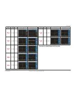
Страница 17: ...o the 4pinOf QP01 03 05 09 11 12 13 work normally Main board Repair replacement Fuse replacement Check LP01 02 04 07 09 12 13 Replace inferior FET SILICON No Yes No No No Refer to a pattern image of T...
Страница 18: ...good Standard Wave pattern image of 1 pin Wave pattern image of 4 pin q QP01 Fig 4 1 FETSLICON MCH5818 w QP03 Fig 4 2 FETSLICON MCH5818 e QP05 Fig 4 3 FETSLICON MCH5818 r QP09 Fig 4 4 FETSLICON MCH58...
Страница 19: ...bleshooting Position of Replacement part Names Of good Standard Wave pattern image of 1 pin Wave pattern image of 4 pin y QP12 Fig 4 6 FETSLICON MCH5818 u QP13 Fig 4 7 FETSLICON MCH5818 Table 4 2 Test...
Страница 20: ...RZ30 RZ31 CP35 CV11 CP36 CV12 CV13 CP38 CV14 RP75 CV15 1103 001416 ICD02 RP76 CV16 CV17 CV18 CV19 D J 0 1 CP43 CP44 CV20 CV21 CV22 CV23 CD95 RS12 CP51 CZ18 CP55 CP56 CP57 CP59 CP60 DP01 RS52 RA09 QS01...
Страница 21: ...S02 BN06 RS07 RJ09 RA16 LV11 LV12 RJ10 RJ11 RJ12 RN01 CD01 RA17 RN02 CD02 RN03 CD03 RN04 RN05 New Part 3711 006788 CNJ01 RN06 RN07 3711 006499 CNJ03 QZ21 Q120 RP01 RP02 RP03 RP04 RP05 RP06 RP07 RP08 R...
Страница 22: ...16 RP53 RP54 RP55 CP19 CD61 LA01 RP56 CD62 LA02 RP57 L A 0 3 RP58 CD64 RP59 CD65 New Part 3708 002 CNZ01 CD67 CD68 CP21 CP22 CP23 RP60 CP24 RZ24 RP61 CP25 RZ25 RP62 CP26 RZ26 CP27 CP28 CP29 CD72 CD73...
Страница 23: ...0 K o h m X X R D 1 0 1 R D 1 0 4 N T S C P A L X X 0 o h m 1 0 0 K o h m 1201 002413 1009 001010 R N 2 0 ICN02 R N 1 9 L A 0 4 10K MAX9502GELT RN1104 0 100K 0 100K 0 MCH5818 4 7uH 0 S29GL064N90TFI040...
Страница 24: ...k normally Check ICS01 Replace ICS02 No Yes A Does an output of ICS02 6Pin work normally No Yes Does an output of QP01 02 04 07 09 12 13 1pin work normally No Yes Replace ICS01 Normal Refer to Wave pa...
Страница 25: ...tronics 4 Troubleshooting Position of Replacement part Names Of good Specification Wave Form q ICS012 16 Pin IC MICOM UPD 78F0535GA w ICS02 6 Pin IC POSI FIXED REG S 8424A Table 4 3 Test Point Wave Pa...
Страница 26: ...SC PAL 100K 100K X X VB AD41 01181A Rev PV MX20 PJ CS31 RS72 RS71 RJ31 RJ32 R J 3 3 1205 002877 100nF 1K 10nF 1M 10nF 22K 3 3K 10nF 0 0 0 100nF 0 10nF 100nF 32 768KHz 47 470nF 10nF 100K 10nF 100K AK46...
Страница 27: ..._Out OK ICA02 No 6 Change AV_Jack Check Replace Video AMP ICA02 No 4 6 No Yes No Yes Checking Multi AV Jack CNS04 Pin Number AV JACK Not inserted Inserted POS 1 A R_OUT 0 V 0 V POS 2 GND 0 V 0 V POS 3...
Страница 28: ...60 RS36 RM03 R D 1 0 1 R D 1 0 4 S C L X X 0 o h m 1 0 0 K o h m 1201 002413 1009 001010 L A 0 4 MAX9502GELT RN1104 MCH5818 S29GL064N90TFI040 22uH 1K A3212ELH 100K 100K 100K 150K 0 220K 120K 150K 220K...
Страница 29: ...ed to QP05 Pin4 Is 12V transited to QP23 Pin3 Change CAMERA ASSY Check ICP01 Check QP23 No Yes No No Check QP05 Is 7 5V transited to QP22 Pin6 Check QP22 No Yes Yes Yes Refer to a pattern image of Fig...
Страница 30: ...CM24 CM25 CS01 CM26 CS02 CM27 CS03 RS07 RS08 NTSC PAL 100K 100K X X VB AD41 01181A Rev PV MX20 PJ BDP01 CP03 CS31 RS72 RS71 R J 3 3 100nF 1K 10nF 1M 22K 3 3K 10nF 0 0 0 100nF 0 10nF 100nF 32 47 470nF...
Страница 31: ...CM25 CS01 CM26 CS02 CM27 CS03 RS07 RS08 NTSC PAL 100K 100K X X VB AD41 01181A Rev PV MX20 PJ BDP01 CP03 CS31 RS72 RS71 RJ31 RJ32 R J 3 3 1205 002877 100nF 1K 10nF 1M 10nF 22K 3 3K 10nF 0 0 0 100nF 0...
Страница 32: ...CS01 CM26 CS02 CM27 CS03 RS07 RS08 NTSC PAL 100K 100K X X VB AD41 01181A Rev PV MX20 PJ BDP01 CP03 CS31 RS72 RS71 RJ31 RJ32 R J 3 3 1205 002877 100nF 1K 10nF 1M 10nF 22K 3 3K 10nF 0 0 0 100nF 0 10nF 1...
Страница 33: ...ck serial port of LCD control CNL01 18 20pin Change Assy LCD 1 Check FPC LCD 2 Check CNJ02 3 6pin voltage of main board 3 Check QP51 QP15 of Main board No Yes No No Input signal in CNL02 CNL03 pin nor...
Страница 34: ...03 CL04 CL05 CL06 CL07 CL08 CL09 CL10 CL11 CL12 CL13 CL14 CL15 ICL01 RL01 RL02 RL03 RL04 82 15K 22K 33K 47K 82K 220K 3 7 0 8 0 0 2 2 2 4 3708 002188 1000nF 1000nF 1000nF 4700nF 1000nF 1000nF 1000nF 10...
Страница 35: ...Are DP DM of IC907 8 7pin Level 0 5V Check IC907 10pin VCC 9pin 0V No Does the Clock of ICD01 Work nor mally XD02 12MHz Check XD02 No Does ICD01 NIKE Work normally Replace ICD01 or Main B d No Yes Ye...
Страница 36: ...001460 RS36 RS37 RS38 N T S C P A L R D 0 7 R D 0 8 0 o h m 1 0 0 K o h m X X R D 1 0 1 R D 1 0 4 N T S C P A L X X 0 o h m 1 0 0 K o h m 1201 002413 1009 001010 L A 0 4 10K MAX9502GELT RN1104 0 0 0...
Страница 37: ...Samsung Electronics 4 21 Troubleshooting q USB_DET RJ07 w IC907 1 2 Pin USB_DP DM e IC907 7 8 Pin USB_DP DM r XD02 USB 12MHz Fig 4 15...
Страница 38: ...Troubleshooting 4 22 Samsung Electronics M E M O...
Страница 39: ...ed View and Parts List 5 1 5 1 Ass y Chassis 5 2 5 2 Ass y Left 5 4 5 3 Ass y Right 5 6 5 4 Ass y Camera 5 8 5 5 Ass y Holder battery 5 9 5 6 Ass y Top 5 10 5 7 Ass y Front 5 11 5 8 Electrical Parts L...
Страница 40: ...sung Electronics 5 1 Ass y Chassis S N A P001 W287 T1 7 X 4W W129 M1 7 X 4W W377 M1 7 X 4B W287 T1 7 X 4W W287 T1 7 X 4W W287 T1 7 X 4W W287 T1 7 X 4W W287 T1 7 X 4W W377 M1 7 X 4B W129 M1 7 X 4W ASSY...
Страница 41: ...Parts List Loc No Parts No Description Specification Q ty SNA Remark P001 AD92 00579G ASSY PCB MAIN MX20 PJ VP MX20 EDC PAL EN 1 SA W129 6001 001719 SCREW MACHINE CH M1 7 L4 NI PLT 3 SA W287 6003 001...
Страница 42: ...9 VS006 P004 C1066 C349 L0533 C827 VS109 C441 PAD BUTTON L006 L013 W377 M1 7 X 4B W371 T1 7 X 4B INLAY LEFT PAD SPEAKER PAD LEFT PAD LEFT BUTTON EASY CASE LEFT C846 L014 L015 P275 W371 T1 7 X 4B C146...
Страница 43: ...ND DISPLAY MX20 SUS30 1 SA FL609 AD97 16203A ASSY FPC LCD MX20 PJ SC MX20C ASSY FPC L 1 SA L006 AD61 03677B CASE LCD TOP MX20 PC ABS T1 5 W60 1 SA L013 AD61 03678B CASE LCD BOTTOM MX20 PC ABS T1 5 1 S...
Страница 44: ...cs 5 3 Ass y Right P319 W371 T1 7 X 4B W287 T1 7 X 4B W127 T1 7 X 3B W127 T1 7 X 3B C069 C011 C635 W371 T1 7 X 4B C0022 W371 T1 7 X 4B C206 C309 C651 C1069 C081 ASSY BELT GRIP CASE GRIP OUT SPRING WAS...
Страница 45: ...B POWER MX20 PC ABS T1 W12 L6 NULL 1 SA C1069 AD61 03671A HOLDER SHAFT DOOR MX20 PC ABS T1 2 W11 L 1 SA C206 AD61 03693A BRACKET RIGHT MX20 SUS304 T0 8 W30 L40 1 SA C309 AD64 02285A BUTTON REC MX20 PC...
Страница 46: ...N A C201 AD61 03688A BRACKET LENS MX20 SUS304 T0 5 W79 L58 1 SA C314 AD97 15560A ASSY CCD VP MX20 MX20 PJ PAL 1 SA C594 AD61 02357A PLATE CCD DRAGON2 PJ AL T1 W21 L25 1 SA P052 AD67 00369A LENS FILTER...
Страница 47: ...8 1 SA C1013 AD64 01671A KNOB LOCKER BATTERY MX10 PC ABS T7 W8 1 SA C1019 AD61 02901A SPRING ETC LOCK BATTERY MX10 SUS 0 2 1 SA C1026 AD61 03706A SPRING ETC BATTERY COIL MX20 SUS 0 35 11 1 SA C1072 AD...
Страница 48: ...15 1 SA C041 AD61 03680A CASE REAR MX20 PC ABS T1 5 W60 L25 NULL 1 SA C1068 AD64 02284A BUTTON MODE MX20 PC ABS W12 L6 NORMAL 1 SA C1073 AD97 16202A ASSY FPC MODE MX20 PJ SC MX20C ASSY FPC 1 SA C822 A...
Страница 49: ...NOB COVER LENS HOLDER KNOB C208 P121 C1045 W206 M1 7 X 3B W398 M1 7 X 4B S N A S N A S N A S N A S N A S N A S N A S N A S N A S N A S N A S N A C062 AD63 03017B COVER FRONT MX20 WHITE 1 50 50 1 SA C1...
Страница 50: ...CD48 2203 003039 C CER CHIP 0 008nF 0 25pF 50V C0G 1 SA CD49 2203 002709 C CER CHIP 100nF 80 20 16V Y5V 1 SA CD51 2203 002709 C CER CHIP 100nF 80 20 16V Y5V 1 SA CD53 2203 002709 C CER CHIP 100nF 80 2...
Страница 51: ...CHIP 0 01nF 0 5pF 50V C0G 1 1 SA CS02 2203 003039 C CER CHIP 0 008nF 0 25pF 50V C0G 1 SA CS03 2203 005627 C CER CHIP 470nF 10 10V X5R 1608 1 SA CS04 2203 002709 C CER CHIP 100nF 80 20 16V Y5V 1 SA CS...
Страница 52: ...07 0501 000225 TR SMALL SIGNAL 2SC4617 NPN 200mW 1 SA QZ21 0504 001025 TR DIGITAL DTC143EE NPN 150mW 4 7 1 SA RA09 2007 000171 R CHIP 0ohm 5 1 16W TP 1005 1 SA RA10 2007 000162 R CHIP 100Kohm 5 1 16W...
Страница 53: ...01 2007 007318 R CHIP 1Kohm 1 1 16W TP 1005 1 SA RP02 2007 007312 R CHIP 20Kohm 1 1 16W TP 1005 1 SA RP03 2007 007142 R CHIP 10Kohm 1 1 16W TP 1005 1 SA RP04 2007 007309 R CHIP 12Kohm 1 1 16W TP 1005...
Страница 54: ...DC 20mA 160gf 4 5 1 SA SWS02 3404 001216 SWITCH TACT 12V DC 20mA 160gf 4 5 1 SA SWS03 3404 001216 SWITCH TACT 12V DC 20mA 160gf 4 5 1 SA XD01 2801 004164 CRYSTAL SMD 12MHZ 50PPM 28 ACI 7P 1 SA XD02 28...
Страница 55: ...5 1 SA RCH11 2007 008596 R CHIP 0 1ohm 1 1 4W TP 3216 1 SA RCH12 2007 007318 R CHIP 1Kohm 1 1 16W TP 1005 1 SA RCH13 2007 007132 R CHIP 15Kohm 1 1 16W TP 1005 1 SA RCH14 2007 000148 R CHIP 10Kohm 5 1...
Страница 56: ...Exploded Views and Parts List 5 18 This Document can not be used without Samsu ng s authorization Samsung Electronics M E M O...
Страница 57: ...6 PCB Diagrams 6 1 Wiring Diagram 6 2 6 2 Main PCB 6 3 6 3 LCD PCB 6 8 6 4 Rear PCB 6 8 6 5 CCD PCB 6 9 6 6 Top PCB 6 9 6 7 LCD FPC 6 10 6 8 Mode FPC 6 10 Samsung Electronics 6...
Страница 58: ...6 Samsung Electronics PCB Diagrams 6 1 Wiring Diagram...
Страница 59: ...RS37 RS38 N T S C P A L R D 0 7 R D 0 8 0 o h m 1 0 0 K o h m X X R D 1 0 1 R D 1 0 4 N T S C P A L X X 0 o h m 1 0 0 K o h m 1201 002413 1009 001010 R N 2 0 ICN02 R N 1 9 L A 0 4 10K MAX9502GELT RN1...
Страница 60: ...60 RS36 RM03 RS37 RS38 N T S C P A L R D 0 7 R D 0 8 0 o h m 1 0 0 K o h m X X R D 1 0 1 R D 1 0 4 N T S C P A L X X 0 o h m 1 0 0 K o h m 1201 002413 1009 001010 R N 2 0 ICN02 R N 1 9 L A 0 4 10K MAX...
Страница 61: ...8 NTSC PAL 100K 100K X X VB AD41 01181A Rev PV MX20 PJ BDP01 CP03 CS31 RS72 RS71 RJ31 RJ32 R J 3 3 1205 002877 100nF 1K 10nF 1M 10nF 22K 3 3K 10nF 0 0 0 100nF 0 10nF 100nF 32 768KHz 47 470nF 10nF 100K...
Страница 62: ...5 Fig 4 3 FETSLICON MCH5818 r QP09 Fig 4 4 FETSLICON MCH5818 t QP11 Fig 4 5 FETSLICON MCH5818 Position of Replacement part Names Of good Standard Wave pattern image of 1 pin Wave pattern image of 4 pi...
Страница 63: ...41 01181A Rev PV MX20 PJ BDP01 CP03 CS31 RS72 RS71 RJ31 RJ32 R J 3 3 1205 002877 100nF 1K 10nF 1M 10nF 22K 3 3K 10nF 0 0 0 100nF 0 10nF 100nF 32 768KHz 47 470nF 10nF 100K 10nF 100K AK4642EN 100nF 10uF...
Страница 64: ...7 0 8 0 0 2 2 2 4 3708 002188 1000nF 1000nF 1000nF 4700nF 1000nF 1000nF 1000nF 1000nF 1000nF 1000nF 1000nF 1000nF 1000nF 100nF 10nF MRUS51S 1209 001585 1 5K 100 1K 3 3K REV R00 LCD PCB MX20 PJ CNL01 C...
Страница 65: ...TOP REV 00 A R C H 2 5 Q C H 2 5 0504 000168 1201 001376 3708 002173 AD43 00181A M A N U A L 10nF 10nF 100nF 10uF VEC2819 10nF RN1104 RN1104 2SB1121 2SB1121 RN1104 RN1104 RN1104 EMD3 EMD3 EMX2 0401 0...
Страница 66: ...ams 6 7 LCD FPC COMPONENT SIDE CONDUCTOR SIDE CNFL02 3711 006813 CNFL02 6 8 MODE FPC COMPONENT SIDE CONDUCTOR SIDE LEDMD1 LEDMD2 SWMD3 RMD1 CR01 CNMD1 0 1 0 4 0601 002037 0601 002037 3404 001312 3708...
Страница 67: ...PC 7 19 This Document can not be used without Samsung s authorization 7 Samsung Electronics For schematic Diagram Resistors are in ohms 1 8W unless otherwise noted Note Do not use the part number show...
Страница 68: ...ICC01 CCD ICX64 1 ICD11 CDS AGC ADC VSP2582RHN ICZ01 M Driver uPD168104 ICC02 CCD V Driver ICM02 DDR1 64MB HYB25DC512160 ICM01 NOR 8MB S29GL064N ICN02 NAND FLASH K9HCG08U1M 48MHz 108MHz 12bit SPI 2 IC...
Страница 69: ...ion q Digital Camcorder technology This feature allows a moving picture to be compressed in MPEG4 and saved in external Memory card Also it decompresses the compressed file saved in external Memory ca...
Страница 70: ...ument can not be used without Samsung s authorization Samsung Electronics Schematic Diagrams 7 3 DC DC Main PCB q 1Pin q 4Pin w 1Pin w 4Pin e 1Pin e 4Pin r 1Pin r 4Pin t 1Pin t 4Pin y 1Pin y 4Pin u 1P...
Страница 71: ...03 Fig 4 2 FETSLICON MCH5818 e QP05 Fig 4 3 FETSLICON MCH5818 r QP09 Fig 4 4 FETSLICON MCH5818 t QP11 Fig 4 5 FETSLICON MCH5818 Position of Replacement part Names Of good Standard Wave pattern image o...
Страница 72: ...ion Samsung Electronics Schematic Diagrams 7 4 MICOM Main PCB q 2Pin q 12Pin w 6Pin q ICS01 2 12Pin w ICS02 6Pin These are the waveforms of VP MX20 MX20H MX20P MX20R MX20C MX20CH MX20CN Caution There...
Страница 73: ...Schematic Diagrams Samsung Electronics This Document can not be used without Samsung s authorization 7 7 5 AFE Main PCB...
Страница 74: ...7 This Document can not be used without Samsung s authorization Samsung Electronics Schematic Diagrams 7 6 Motor Main PCB...
Страница 75: ...Schematic Diagrams Samsung Electronics This Document can not be used without Samsung s authorization 7 7 7 DSP Digital Signal Processor Main PCB VIDEO AUDIO...
Страница 76: ...7 10 This Document can not be used without Samsung s authorization Samsung Electronics Schematic Diagrams 7 8 Memory Main PCB...
Страница 77: ...Schematic Diagrams Samsung Electronics This Document can not be used without Samsung s authorization 7 11 7 9 Storage Main PCB...
Страница 78: ...7 12 This Document can not be used without Samsung s authorization Samsung Electronics Schematic Diagrams 7 10 Audio Main PCB VIDEO AUDIO...
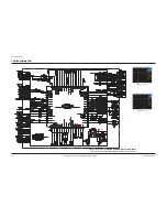
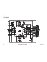
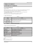
Страница 79: ...Schematic Diagrams Samsung Electronics This Document can not be used without Samsung s authorization 7 13 7 11 Jack Main PCB VIDEO AUDIO...
Страница 80: ...7 14 This Document can not be used without Samsung s authorization Samsung Electronics Schematic Diagrams 7 12 LCD LCD PCB VIDEO...
Страница 81: ...Schematic Diagrams Samsung Electronics This Document can not be used without Samsung s authorization 7 15 7 13 Rear Rear PCB...
Страница 82: ...7 16 This Document can not be used without Samsung s authorization Samsung Electronics Schematic Diagrams 7 14 CCD CCD PCB...
Страница 83: ...Schematic Diagrams Samsung Electronics This Document can not be used without Samsung s authorization 7 17 7 15 Top Top PCB...
Страница 84: ...7 18 This Document can not be used without Samsung s authorization Samsung Electronics Schematic Diagrams 7 16 LCD FPC LCD FPC...
Страница 85: ...Schematic Diagrams Samsung Electronics This Document can not be used without Samsung s authorization 7 19 7 17 Mode FPC Mode FPC Refer to a pattern image of Page 7 17...
Страница 86: ...7 20 This Document can not be used without Samsung s authorization Samsung Electronics Schematic Diagrams M E M O...
Страница 87: ...n data up and menu up Changes data and mode in the admin mode Move the cursor in the admin mode DOWN Tele button data down and menu down Menu Key It is used to escape the admin mode 4 How to set the c...
Страница 88: ...n mode to the highest menu by pressing the BACK After finishing the control escape from the control mode to the highest menu by pressing the Menu Key To store the set value reset the power q MENU butt...
Страница 89: ...EXIT 2008 06 20 LAST EEPROM TABLE EEPROM ADJUST EEPROM ALL IN IT EEPROM DEFAULT SET EEPROM CAM IN IT BACK 22 1311 Jun 20 2008 MENU EXIT 2008 06 20 LAST EEPROM TABLE Push the OK Button Fig 8 2 If you...
Страница 90: ...lance 5100K 1 HALL adjust q The camera should be in E E mode Video Record w Connect the AV cable to Input port of Monitor or TV e After entering the Admin mode press the OK button in Camera Adjust men...
Страница 91: ...rce the zoom and focus lens when setup y Adjustment completed displays after finishing Lens 3M Adjust Caution For whole zoom range it shall be in focus The location of a focus lens is moving depending...
Страница 92: ...to the center of display at the vector scope u Adjustment completed displays after finishing 3100K Adjust 6 Auto White Balance adjust 5100K q The camera should be in E E mode Video Record w Prepare th...
Страница 93: ...to upgrade the MX20 Firmware I ll send the new software Image There are two files nike bin micom bin 1 First please copy this file to SD Card root Picture Fig 8 4 2 Turn on the MX20 3 Insert the SD C...
Страница 94: ...can see the screen like that Update to MICOM F W Fig 8 8 8 Start update done And power off automatically Fig 8 9 9 turn on the MX20 You ll check the software version menu Left Key setting Up Key Vers...
Страница 95: ...Update is OK on the monitor Update is successful 3 Troubleshooting a When the SDHC MMC fails to be recognized q Remove the SDHC MMC and turn the power off and on w Insert the SDHC MMC card and change...
Страница 96: ...the camcorder is turned on If the message disappears and the Admin mode screen appears again on the monitor it means that the update is finished successfully Step 3 q It will restart automatically af...