Alignment and Adjustments
4-14
Samsung Electronics
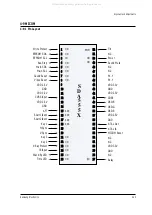
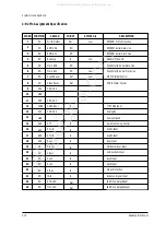
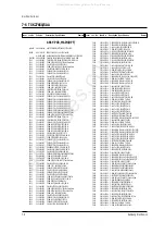
4-9-2 Pin Assignment Specification
DESCRIPTION
EEPROM Write Protection
EEPROM Serial Data Line
EEPROM Serial Clock Line
Disable Micom IIC
Peripheral IC Serial Data Line
Peripheral IC Serial Clock Line
MSP IC Initial Control
VDP IC Initial Control
TTX CVBS Input
Analog B+
Analog Ground
Auto Fine Tuning Control
Scart1 Ident
Scart2 Ident
Key1 Input
Horizontal Sync Input
Vertical Sync Input
Key3 Input
Key2 Input
X-Ray Protection
Remocon Signal Input
LED Drive Output(Red)
LED Drive Output(Green)
PIN NO
1
2
3
4
5
6
7
8
9
10
11
12
13
14
15
16
17
18
19
20
21
22
23
24
25
26
FUNCTION
I/O
I/O
I/O
I/O
I/O
I/O
I/O
I/O
Vdd
GND
Vdd
CVBS
Vdd
GND
ADC
ADC
ADC
ADC
HS
VS
I/O
I/O
I/O
I/O
I/O
I/O
ASSIGN
Write Protect
ROM SDA
ROM SCL
Bus Stop
Main SDA
Main SCL
Sound Reset
Video Reset
VDD 2.5V
VDD 3.3V
CVBS Input
VDD 2.5V
AFT
SC1-ID
SC2-ID
Key1
H-Sync
V-Sync
Key3
Key2
X-Ray
IR-In
STD-LED
TIM-LED
IN/OUT
Out
I/O
I/O
In
I/O
I/O
Out
Out
In
In
In
In
In
In
In
In
In
In
In
Out
Out
ACTIVE H/L
Low
Low
Low
Low
All manuals and user guides at all-guides.com
all-guides.com
Содержание TXK2750X/XAC
Страница 12: ...3 2 Samsung Electronics MEMO All manuals and user guides at all guides com ...
Страница 28: ...4 16 Samsung Electronics MEMO All manuals and user guides at all guides com ...
Страница 53: ...8 2 Block Diagram Schematic Diagrams 8 2 Samsung Electronics All manuals and user guides at all guides com ...
Страница 55: ...9 2 Samsung Electronics MEMO All manuals and user guides at all guides com ...
Страница 60: ...10 5 POWER W O EW Samsung Electronics Schematic Diagrams 10 5 All manuals and user guides at all guides com ...
Страница 62: ...Samsung Electronics 10 7 VIDEO SWITCH Schematic Diagrams 10 7 All manuals and user guides at all guides com ...


