3-20
Samsung Electronics
Disassembly and Reassembly
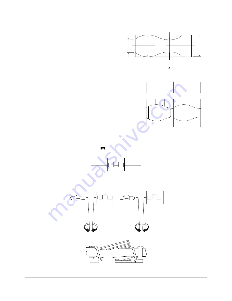
3-5-2 Linearity adjustment
(Guide roller S, T adjustment)
1) Playback the Mono Scope alignment tape (SP mode).
2) Observe the video envelope signal on an oscillo-
scope (triggered by the video switching pulse).
3) Make sure the video envelope waveform (at its
minimum) meets the specification shown in
Fig. 3-5-4.
If it does not, adjust as follows :
Note :
a=Maximum output of the video RF envelope.
b=Minimum output of the video RF envelope at the
entrance side.
c=Minimum output of the video RF envelope at the
center point.
d=Maximum output of the video RF envelope at the
exit side.
4) If the section A in Fig. 3-5-5 does not meet the
speci-fication, adjust the guide roller S up or
down.
5) If the section B in Fig. 3-5-5 does not meet the
speci-fication, adjust the guide roller T up or down.
Fig. 3-5-4 Envelope Waveform Adjustment
a
a b c d
c,b,d/a 63%
b
c
d
Fig. 3-5-5 Adjustment Points
A
B
A
B
H'D SWITCHING
PULSE
ENVELOPE
6) Play back the Mono Scope alignment tape (SP mode).
7) Connect an oscilloscope CH-1 to the Envelope and CH-2 to the H’D SW Pulse for triggering.
8) Turn the guide roller heads with a flat head ( ) driver to obtain a flat video RF envelope as shown in Fig. 3-8.
Fig. 3-5-6 Guide Roller S, T Height Adjustment
IDEAL ENVELOPE
S HEIGHT TOO HIGH
S HEIGHT TOO LOW
T HEIGHT TOO HIGH
T HEIGHT TOO LOW
GUIDE ROLLER S
GUIDE ROLLER T
Содержание TI21B4DF4X
Страница 98: ...Block Diagrams 8 2 Samsung Electronics 8 2 C17A PCB Layout ...
Страница 99: ...9 Wiring Diagram 9 1 C17A Wiring Diagram Wiring Diagram Samsung Electronics 9 1 ...
Страница 101: ...Schematic Diagrams 10 2 Samsung Electronics 10 2 MAIN2 VOC TUNER BOX ...
Страница 102: ...TP07 TP08 TP09 TP10 TP11 Schematic Diagrams 10 3 Samsung Electronics 10 3 MAIN3 VCR A V BLOCK TP01 TP02 TP03 TP04 TP05 ...
Страница 103: ...Schematic Diagrams 10 4 Samsung Electronics 10 4 MAIN4 SWITCHING BLOCK ...
Страница 104: ...Schematic Diagrams 10 5 Samsung Electronics 10 5 MAIN5 OPTION PAL HIFI BLOCK ...
Страница 105: ...Schematic Diagrams 10 6 Samsung Electronics 10 6 MAIN6 OPTION VCR SECAM BLOCK ...
Страница 106: ...Schematic Diagrams 10 7 Samsung Electronics 10 7 POWER FBT ...
Страница 107: ...Schematic Diagrams 10 8 Samsung Electronics 10 8 CRT ...
Страница 108: ...Schematic Diagrams 10 9 Samsung Electronics 10 9 FRONT A V MASTER SW FRONT A V MASTER SW ...


