background image

3 Alignments and Adjustments

3-1

3-1 Required Equipment

The following equipment is necessary for adjusting the monitor:

- Computer with Windows 95, Windows 98, Windows 2000, Windows XP or Windows NT.

- MTI-2055, 2058, or 2059 DDC MANAGER JIG

3-2 Automatic Color Adjustment

To input video, use 16 gray or any pattern using black and white.

1. Select english for OSD language.

2.  Press the "     (Enter/Source)" key for 5 seconds.

3-3 DDC EDID Data Input

1. Input DDC EDID data when replacing AD PCB.

2. Receive/Download the proper DDC file for the model from HQ quality control department.

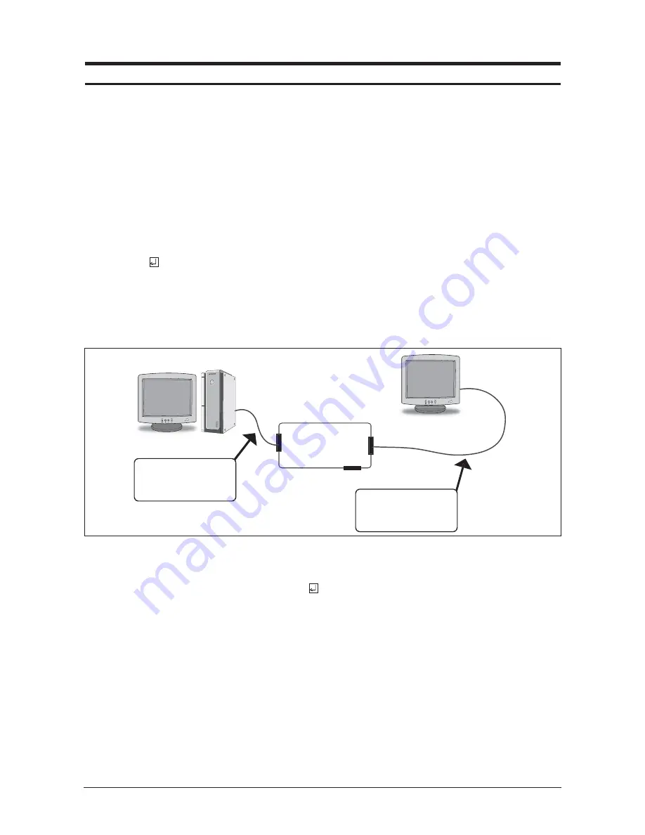
Install the below jig (Figure 1) and enter the data.

3-4 OSD Adjustment When Replacing Panel

1. Adjust brightness and contrast to 0. Then, press the 

(Enter/Source) key for 5 second. 

Service function OSD will appear on screen.

2. Press the + key to place the cursor on the panel. Press the menu key for 5 seconds.

3-5 OSD Adjustment When Replacing Lamp Only

1. Adjust brightness and contrast to 0. Then, press the exit key for 5 seconds. 

Service function OSD will appear on the screen.

2. Press the + key. Select upper lamp and press the menu key for 5 seconds. 

Then, select lower lamp and press the menu key for 5 seconds.

-

Note : Please be sure to read the following instructions for details on service function.

3 Alignments and Adjustments

This section of the service manual explains how to use the DDC MANAGER JIG.
This function is needed for AD board change and program memory (IC201) change.

MTI-2055
DDC Manager

Parallel Connector

(25P Cable)

Connect Monitor

(Signal Cable)

Figure 1.

Содержание SyncMaster 932BF

Страница 1: ...r Fashion Feature LCD Monitor Chassis LPE19DS Model 932BF Integrated UI applied Lustrous Ball Hinge Response Time Accelerator Dynamic Contrast Connectivity Analog 15p Dsub Dual 24p DVI D Power Consumption 38W DPMS under 1 W 230Vac ...

Страница 2: ...Gu Suwon City Gyeonggi Do Korea 443 742 Printed in Korea P N URL http itself sec samsung co kr This Service Manual is a property of Samsung Electronics Co Ltd Any unauthorized use of Manual can be punished under applicable International and or domestic law ...

Страница 3: ...ay not be comfortable to your eyes depending on your taste If this is the case adjust the brightness and con trast by using the OSD menu 2 Text For documentations or works involving heavy text 3 Internet For working with a mixture of images such as text and graphics 4 Game For watching motion pictures such as a game 5 Sport For watching motion pictures such as a sport 6 Movie For watching motion p...

Страница 4: ...his button for auto adjustment Available in Analog mode only 6 Power button Use this button for turn the monitor on and off Power indicator This light glows green during normal operation and blinks green once as the monitor saves your adjustments 10 2 Rear The configuration at the back of the monitor may vary from product to product 1 Power port Connect the power cord for your monitor to the power...

Страница 5: ... sub connector on the back of your monitor 2 2 Using the DVI Digital connector on the video card Connect the DVI cable to the DVI port on the back of your monitor 2 3 Connected to a Macintosh Connect the monitor to the Macintosh computer using the D SUB connection cable 3 Turn on your computer and monitor If your monitor displays an image installation is complete 10 Operating Instructions and Inst...

Страница 6: ...10 Operating Instructions and Installation 10 4 Memo ...

Страница 7: ... 1 Disassembly Cautions 1 Disassemble stand on a flat desk 2 Disconnect the monitor from the power source before disassembly Description Picture Description 1 Place a soft cloth on the desk and place the monitor on the cloth upside down Remove the stand in the direction of the arrow 2 Turn the monitor so the front section is facing upwards Remove the marked parts from the front cover as shown in t...

Страница 8: ... shown in the figure below 1 5 Remove the marked part from the front cover as shown in the figure below Caution Do not lift the front cover over position 1 which may cause damage to it 6 Turn the monitor so the back of it is facing upwards Lift up and remove the back cover 7 Use the jig to remove the shield lamp Be careful Shield ...

Страница 9: ...11 Disassembly and Reassembly 11 3 Description Picture Description LVDS INVERTER FUNCTION 8 Disconnect cables LVDS INVERTER and FUNCTION cable 9 Lift up the LCD panel 10 LCD Panel ...

Страница 10: ...11 Disassembly and Reassembly 11 4 설 설 명 사 사진 설명 11 Remove screws 17 2 screws 19 4 screws Description Picture Description 12 Remove 5 screws 13 Lift up the Bracket Support ...

Страница 11: ...and Reassembly 11 5 설 설 명 사 사진 설명 Description Picture Description 14 Lift up the Main PCB and IB Board 15 Main PCB and IB Board 11 2 Reassembly Reassembly procedures are in the reverse order of disassembly procedures ...

Страница 12: ...ting up or moving the monitor do not lift the monitor upside down while holding only the stand as this may cause the monitor to fall leading to damage or personal injury B Connecting pin C Stand 1 Insert the connecting pin into the stand 2 Stand the screw handles up and tighten the screws firmly by turning them 3 Place the screw handles back down ...

Страница 13: ...monitor upwards at an angle of 5 to 10 so that the base is closer to you than the top Then hold the monitor on the stand by its top parts and push them downwards You can assemble it more easily by pushing it down while wriggling it a little to the left and right 5 When the monitor is assembled correctly the straight groove line at the back of the connecting pin will not be visible when the monitor...

Страница 14: ...iption 1 Place a soft cloth or cushion on the table and place the monitor with the front facing downwards 2 Hold the monitor and lean the stand upwards 3 Hold the monitor and then twist the stand strongly to the left and pull it out 4 Stand the screw handles up and unfasten the screws by turning them ...

Страница 15: ...11 Disassembly and Reassembly 11 9 설 설 명 사 사진 설명 Description Picture Description 5 Remove the connecting pin from the stand ...

Страница 16: ...11 Disassembly and Reassembly 11 10 Memo ...

Страница 17: ...ust brightness and contrast to 0 Then press the Enter Source key for 5 second Service function OSD will appear on screen 2 Press the key to place the cursor on the panel Press the menu key for 5 seconds 3 5 OSD Adjustment When Replacing Lamp Only 1 Adjust brightness and contrast to 0 Then press the exit key for 5 seconds Service function OSD will appear on the screen 2 Press the key Select upper l...

Страница 18: ...service function OSD you will have to power off Figure 2 The example of service function OSD Figure 3 Panel Information Softward Version Checksum The service function OSD is based on a grid of 29 columns x 12 rows The service function OSD consists of panel information software version and MICOM checksum 3 6 2 How to Control Service Function OSD 1 With the panel selected on OSD whenever you press t...

Страница 19: ... panel Ch No increases one step and the panel time information is reset to zero Simultaneously other information is reset to zero Upper Lower lamp Panel cycle Figure 5 6 3 6 4 How to Control Service Function OSD In the case of Upper Lamp or Lower Lamp change After changeing the Upper Lamp or Lower Lamp 1 Select the Upper Lamp or Lower Lamp 2 Press the Menu key within an 5 seconds Then Ch No and ti...

Страница 20: ...ts 3 4 3 7 How to execute DDC 1 3 2 4 5 1 Open file 2 Select Port 1 3 Select DDC file 4 Click Next Button 5 Type in the monitor serial number and press Enter Repeat this step 2 to 5 times in digital inputs after the analog input ...

Страница 21: ...w to execute MCU Code 1 Set the options Manufacture MSTAR Device Type TSUM16_ROM128K_ext_flash Communication Port DSUB15 Analog External Memory PMC25LV010E 2 Click LoadFile button and select the MCU code 3 8 1 Program Setting Config Setting ...

Страница 22: ...3 Alignments and Adjustments 3 6 3 Click Auto Program button 4 If Program and Verify is OK turn off the hard power and than turn on again ...

Страница 23: ...12 PCB Layout 12 1 12 PCB Diagram 12 1 Main PCB Layout ...

Страница 24: ...12 PCB Layout 12 2 Memo ...

Страница 25: ...itor to optimum condition by pushing one key OSD On Screen Display On screen display customer can control the screen easily with this Image Lock This means Fineness adjustment in LCD Monitor the features are Fine and Coarse FINE Fine adjustment is used to adjust visibility by control phase difference COARSE This is a adjustment by tuning with Video colck and PLL clock DVI Digital Visual Interface ...

Страница 26: ...een from the top to the bottom in order is called the Non Interlace method while showing odd lines and then even lines in turn is called the Interlace method The Non Interlace method is used for the majority of monitors to ensure a clear image The Interlace method is the same as that used in TVs Plug Play This is a function that provides the best quality screen for the user by allowing the compute...

Страница 27: ...ower Input 5V Self Raster GND Bi Dr Data SDA H V Sync Not Used DDC Clock SCL Red Green H V Sync Blue GND DDC Return GND GND R GND G GND B DDC Power Input 5V Self Raster GND Bi Dr Data SDA Not Used Not Used DDC Clock SCL Sync on green No Connection 5V_M Self Raster 5V_M Rx0 Rx0 NC No Connection No Connection NC RxC RxC 13 14 15 16 17 18 19 20 21 22 23 24 1 2 3 4 5 6 7 8 9 10 11 12 Rx2 Rx2 GND No Co...

Страница 28: ...emark IBM 640 75 Hz 640x480 800 60 Hz 800x600 800 75 Hz 800x600 1024 60 Hz 1024x768 1024 75 Hz 1024x768 VGA2 70 Hz 720 x 400 VGA3 60 Hz 640 x 480 Table 14 1 Timing Chart 31 469 31 778 3 813 1 589 26 058 0 318 59 940 16 683 0 064 0 794 15 761 0 064 26 175 Negative Negative Separate 37 500 26 667 2 032 3 810 20 317 0 508 75 000 13 333 0 080 0 427 12 800 0 027 31 500 Negative Negative Separate 37 879...

Страница 29: ...2 x 864 67 500 75 000 108 00 VESA 1280 x 960 60 000 60 000 108 00 VESA 1280 x 1024 63 981 60 020 108 00 VESA 1280 x 1024 79 976 75 025 135 00 If the signal transferred from the computer is the same as the following Preset Timing Modes the screen will be adjusted automatically However if the signal differs the screen may go blank while the power LED is on Refer to the video card manual and adjust t...

Страница 30: ...L02 BN07 00062A EH Panel for 15 Wide TV SEC LTM170EU L01 BN07 00071A EJ Slim design TN SEC LTM170E5 L04 BN07 00072A EK E5 L04 6 bits FRC for IBM SEC LTA220W1 L01 BN07 00074A EL Panel for 22 TV SEC LTM170E6 L02 BN07 00075A EM AMLCD Narrow slim design 17 PVA mode SEC LTM170W1 L01 BN07 00082A EN LTM170W1 L01 ZPD panel SEC LTM170EH L01 BN07 00080A EP LTM170EH L01 ZPD panel SEC LTM170E5 L01 BN07 00081A...

Страница 31: ...B E24 24 panel ZPD code derivation SEC LTM190E4 L01 BN07 00145B E25 AMLCD 19 ZPD Panel code derivation SEC LTM240W1 L03 BN07 00134B E26 24 panel ZPD code derivation SEC LTM150XO L01 BN07 00164A E27 AMLCD 15 XO L01 new panel development SEC LTM150XO L01 BN07 00164B E28 AMLCD 15 XO L01 ZPD code derivation SEC LTM170EU L11 BN07 00160B E29 AMLCD 17 NEW panel code derivation SEC LTA320W2 L01 BN07 00172...

Страница 32: ...ode SEC LTM190M2 L02 BN07 00287A STZ AMLCD 19 TN Wide High brightness NEW Panel Code SEC LTA400WS L01 BN07 00246A SPZ Display LCD Div 07AH SEC LTA460WS L01 BN07 00311A SPZ SEC LTM190E4 L31 BN07 00316A SPZ SEC LTM170EX L31 BN07 00278A STZ AMLCD LTM170EX L31 ZPD SEC LTA460HS LH1 BN07 00291A SPZ AMLCD 46 16 9 FHD 60Hz 8bit SPVA 92 SEC LTA320WT LF1 BN07 00323A SPZ SEC LTA460WT L02 BN07 00284A SPZ AMLC...

Страница 33: ...D190MEN2 A BN07 00341A NTZ TORISAN TM150XG 22L03 A BN07 00021A RA TORISAN TM150XG 26L06 BN07 00042A RB TORISAN TM181SX 76N01 BN07 00048A RC TORISAN TM150XG 26L06 BN07 00059A RD 15 XGA TN MODE ZPD TORISAN TM290WX 71N31 BN07 00063A RE RS24NS TORISAN 29 NEW PANEL TORISAN TM396WX 71N31 BN07 00064A RF RS24NS TORISAN 40 NEW PANEL TORISAN TM150XG 26L09 BN07 00073A RG Panel for 15 TV TORISAN TM150XG 26L10...

Страница 34: ...076A AB AU 17 Panel Narrow slim design ACER M170EN05 BN07 00102A AC ZPD Panel code ACER M190EN02 BN07 00170A AMH AU Monitor 19 new panel development P19 1S ACER M190EN02 BN07 00170B AMZ AU 19 ZPD code derivation ZPD ACER M170EN06 BN07 00171A ATH AU Monitor 17 New panel development ACER T260XW01 BN07 00163A AMZ AU 26 new panel development NF26EO ACER A201SN01 BN07 00177A ATZ AU TV panel 20 1 TN SVG...

Страница 35: ...6B CQ HIGHLAND 17 LOW PANEL ZPD derivation panel CHIMEI M170E6 L05 BN07 00152A CR CMO 17 new panel development code CHIMEI M170E6 L05 BN07 00152B CS CMO 17 ZPD panel code derivation CHIMEI M150X4 L06 BN07 00137B CT Chimei 15 Narrow Slim panel ZPD derivation CHIMEI M170E5 L05 BN07 00165A CTH CMO 17 new panel development code GOYA2 PJT CHIMEI M170E5 L05 BN07 00165B CTZ CMO 17 ZPD panel GOYA2 PJT CHI...

Страница 36: ...Memo 14 Reference Infomation 14 12 ...

Страница 37: ...on Horizontal 1280 Pixels Vertical 1024 Pixels Input Signal Analog Digital Input Sync Signal Seperate H V sync Composite H V Sync on Green Level TTL level Maximum Pixel Clock rate 135 MHz Active Display Horizontal Vertical 376 32 H x 301 06 V mm AC power voltage Frequency AC 90 264 VAC 60 50 Hz Power Consumption 38W Max Dimensions Set W x D x H 14 8 x 7 0 x 15 0 inch 376 0 x 177 0 x 380 0 mm Weigh...

Страница 38: ...ode Input Signal Sync Signal Power Consumption Normal Power Saving 5ms 700 1 Support Deleted Magic Zone 2ms G to G 1000 1 2000 1 Dynamic Contrast Support Deleted Magic Zone Response Time Contrast Ratio Magic Color 38W 1W 38W 1W Analog Digital Seperate Composite Sync on Green Analog Digital Seperate Composite Sync on Green 1280 x 1024 60 Hz 1280 x 1024 75 Hz 1280 x 1024 60 Hz 1280 x 1024 75 Hz LPE1...

Страница 39: ...uide BH68 00376L BH68 00633A BN59 00585F BN39 00244B 3903 000042 BN39 00246F Sold separatelys Warranty Card Not available in all locations User s Guide Monitor Driver Natural Color software MagicTune software D Sub 15 Pin Cable Power Cord DVI Cable 2 4 Option Specification ...

Страница 40: ...2 Product Specifications 2 4 Memo ...

Страница 41: ...per DC1 8V appear at Pin 2 of IC602 Check IC602 and related circuit No Notes 1 Before troubleshooting setup the PC s display as below Resolution 1280 x 1024 H frequency 64 kHz V frequency 60 Hz 2 If no picture appears make sure the power cord is correctly connected 3 Check the following circuits No raster appears Function PBA Main PBA I P PBA 5V develop but no screen Main PBA 5V does not develop I...

Страница 42: ...14 and R118 Check input part Yes No Is there Hsync Vsync waveform at Pin 32 33 of IC200 Check IC200 and related circuit No 2 3 Yes Does the output signal appear at Pin 17 20 22 27 of CN400 Check CN400 and related circuit No Yes There are DC 5V at Pin 1 2 and 3 of CN400 Check PANEL_EN SIGNAL at R223 is High On High and BL_EN signal at R601 ON Low is Low No Yes Replace LCD Panel ...

Страница 43: ...4 Troubleshooting 4 3 1 WAVEFORMS 2 3 ...

Страница 44: ...tion and power Yes No Is there R G B input at R100 R101 R102 R106 and R108 Check input part Yes No Does the output signal appear at Pin 17 20 22 27 of CN400 Check IC400 and related circuit No Yes There are DC 5V at Pin 1 2 and 3 of CN400 Check the PANEL_EN signal at R222 and BL_EN signal at R603 No Yes Replace LCD Panel 6 5 4 ...

Страница 45: ...4 Troubleshooting 4 5 1 WAVEFORMS 5 4 6 ...

Страница 46: ...4 Troubleshooting 4 6 Memo ...

Страница 47: ... Parts List 5 1 5 Exploded View and Parts List You can search for updated part codes through ITSELF web site URL http itself sec samsung co kr 5 1 LS19PEDSFU EDC Exploded View T0003 M0215 M0174 T0514 M0006 M0013 M0013 ...

Страница 48: ...15 BN07 00474A LCD PANEL M190EG02 V4 Haydn 6bit Hi FRC 1 S A M0174 BN44 00124J IP BOARD IP 35155A PV Pebble 3 0 5 0mA 1 S A T0514 BN61 02784A BRACKET SUPPORT PEBBLE SPTE 0 3 1 S N A M0006 BN96 04145A ASSY SHIELD P COVER PEBBLE19 SECC T0 8 1 S N A M0013 BN96 06492A ASSY COVER P REAR LS19PE AUO ABS HB B 1 S A M0013 BN96 04150D ASSY STAND P BAR PEBBLE17 ABS HB BK2 1 S A ...

Страница 49: ...S A 7 C120 2203 000189 C CER CHIP 100nF 80 20 25V Y5V 1608 3 S A 7 C120 2203 000189 C CER CHIP 100nF 80 20 25V Y5V 1608 1 S A 7 C120 2203 000189 C CER CHIP 100nF 80 20 25V Y5V 1608 1 S A 7 PCB BN41 00793B PCB SUB FUNCTION Pebble FR 1 1 1 1 1 6 8 1 S N A 4 BN94 01310C ASSY PCB MISC SEDA POWER BN96 PABBLE 1 S N A 5 L0405 0601 001896 LED SMD BLUE 1 6x0 8x0 4mm 470 1 6x0 8x0 1 S A 5 L0405 0601 001896 ...

Страница 50: ...SOD 323 T 1 S A 4 D0254 0404 001020 DIODE SCHOTTKY BAT54C 30V 200mA SOT 23 T 1 S A 4 D0254 0404 001020 DIODE SCHOTTKY BAT54C 30V 200mA SOT 23 T 1 S A 4 ZD200 0406 001061 DIODE TVS MMQA5V6T3 5 32 5 6 5 88V 24W S 1 S A 4 ZD201 0406 001061 DIODE TVS MMQA5V6T3 5 32 5 6 5 88V 24W S 1 S A 4 ZD202 0406 001061 DIODE TVS MMQA5V6T3 5 32 5 6 5 88V 24W S 1 S A 4 Q201 0501 000445 TR SMALL SIGNAL KTC3875S Y NPN...

Страница 51: ...0 2007 000084 R CHIP 4 7Kohm 5 1 10W TP 1608 1 S A 4 R110 2007 000084 R CHIP 4 7Kohm 5 1 10W TP 1608 1 S A 4 R110 2007 000084 R CHIP 4 7Kohm 5 1 10W TP 1608 1 S A 4 R110 2007 000084 R CHIP 4 7Kohm 5 1 10W TP 1608 1 S A 4 R110 2007 000084 R CHIP 4 7Kohm 5 1 10W TP 1608 1 S A 4 R110 2007 000090 R CHIP 10Kohm 5 1 10W TP 1608 1 S A 4 R110 2007 000090 R CHIP 10Kohm 5 1 10W TP 1608 1 S A 4 R110 2007 000...

Страница 52: ... X7R 1608 1 S A 4 C120 2203 005005 C CER CHIP 100nF 10 16V X7R 1608 1 S A 4 C120 2203 005005 C CER CHIP 100nF 10 16V X7R 1608 1 S A 4 C120 2203 005005 C CER CHIP 100nF 10 16V X7R 1608 1 S A 4 C120 2203 005005 C CER CHIP 100nF 10 16V X7R 1608 1 S A 4 C120 2203 005005 C CER CHIP 100nF 10 16V X7R 1608 1 S A 4 C120 2203 005005 C CER CHIP 100nF 10 16V X7R 1608 1 S A 4 C120 2203 005005 C CER CHIP 100nF ...

Страница 53: ... 10V Y5V 3216 1 S A 4 C120 2203 005437 C CER CHIP 10000nF 80 20 10V Y5V 3216 1 S A 4 C120 2203 005437 C CER CHIP 10000nF 80 20 10V Y5V 3216 1 S A 4 C120 2203 005437 C CER CHIP 10000nF 80 20 10V Y5V 3216 1 S A 4 C120 2203 005437 C CER CHIP 10000nF 80 20 10V Y5V 3216 1 S A 4 C120 2203 006336 C CER CHIP 10000nF 10 25V X5R 3216 1 S A 4 C435 2402 001042 C AL SMD 100uF 20 16V GP TP 6 6x6 6x5 4 1 S A 4 C...

Страница 54: ... S A 3 M0081 6003 000282 SCREW TAPTITE BH B M3 L8 ZPC BLK SW 4 S A 3 T0524 6902 000389 BAG PE HDPE NITRON HDPE T0 015 T0 5 T0 0 1 S N A 3 CIS4 BN61 01717A HOLDER STAND BIZET NI PLT CH M4 L11 5 1 S A 3 BN61 02785A BRACKET STAND BODY PEBBLE SECC 0 8 1 S N A 3 CCM1 BN63 02183C COVER SHEET Rhcm PE Vinyl T0 05 200mm 20 0 3 S N A 3 T0004 BN63 02882B COVER STAND BASE PEBBLE ABS 2 6 HB BK26 1 S N A 3 T013...

Страница 55: ...7 Block Diagrams 7 1 7 Block Diagram 7 1 Power Tree ...

Страница 56: ...7 Block Diagrams 7 2 7 2 Main Board Part ...

Страница 57: ...7 3 IP Board Part SMPS Part 7 Block Diagrams 7 3 ...

Страница 58: ...7 4 IP Board Part Inverter Part 7 Block Diagrams 7 4 ...

Страница 59: ...pliances and Underwriters Laboratories UL Publication UL1410 59 7 Figure 1 1 Leakage Current Test Circuit 4 With the unit completely reassembled plug the AC line cord directly into a 120V AC outlet With the unit s AC switch first in the ON position and then OFF measure the current between a known earth ground metal water pipe conduit etc and all exposed metal parts including metal cabinets screwhe...

Страница 60: ...e AC source and turn the power switch ON Connect an insulation resistance meter 500 V to the blades of the AC plug The insulation resistance between each blade of the AC plug and accessible conductive parts see above should be greater than 1 megohm 6 Always connect a test instrument s ground lead to the instrument chassis ground before connecting the positive lead always remove the instrument s gr...

Страница 61: ...ct it from being exposed to moisture Otherwise it may cause a fire or electric shock 5 Make sure to turn the power off and unplug the power cord from the outlet before repositioning the product Also check the antenna cable or the external connectors if they are fully unplugged Damage to the cord may cause fire or electric shock 6 Keep the antenna far away from any high voltage cables and install i...

Страница 62: ...1 Precautions 1 4 Memo ...

Страница 63: ... The Scaler consumes power up to 37mA 1 3 The power to the panel is switched off 2 When the AD board is operating normally 2 1 The maximum power consumption of the panel lamps is described below It may vary depending on the panel manufacturer 19 4 7 5mA 720mVrms 4 5 4 21 6W 2 2 The power consumption of the Panel Control board is as follows 5V 720mA 3 6W 2 3 The power consumption of the Scaler is a...

Страница 64: ...own scaling that are transferred to the panel in the LDVS formats 5 Crystal Oscillator Use one 14 318MHz oscilla tor externally to supply power to both MCU and Scaler at the same time 6 SCALER EEPROM I2C is a two way serial bus of two lines that supports communications across the integrated circuits as well as between FLASH and EEPROM In particular FLASH and Scaler SE656MR LF use the SDR direct bu...

Страница 65: ...13 Circuit Descriptions 13 3 13 1 3 IP BOARD BLOCK POWER Parts 13 1 4 IP BOARD BLOCK INVERTER Parts ...

Страница 66: ...ROTECTION MODE 1 OVP Over Voltage Protection If the Voltage of the series capacitors C10 C15 is over the 2 0V the Inverter latched off See the Picture1 2 OLP Over Load Protection If the inverter output harness is opened No output current the base of the Q1 turns on and chage the C9 ovter 2V and then the Inverter latched off See the Picture2 ...

Страница 67: ...E Yes No 3 pin of FDM0565R Vcc system in normal HIGH Check the Vcc system Yes No 1 pin of FDM0565R Check the drain system Normal Switching Check the output current Check the main switching Check others Harness Inlet Power On No Check the feedback system No Check the protection system No Yes Yes ...

Страница 68: ... 1 and 2 pins of FDM0565R Check Protection Normal 0 6V 0 8V Check the IC drive Check MOSFET Yes No 1 and 2 pins of FDM0565R Check Protection Normal 0 6V 0 8V Check the output current Check the OVP and OLR circuits Check others Power On No Check the feedback system No Check any dimming circuit No Yes Yes ...

Страница 69: ...13 Circuit Descriptions 13 7 13 3 IP BOARD Power Schematic Diagrams ...

Страница 70: ...13 Circuit Descriptions 13 8 13 4 IP BOARD Inverter Schematic Diagrams ...

Страница 71: ...IO GPIO 47 48 GPIO GPIO 49 5 DDCD_SDA 50 GPIO GPIO_P24 PWM2 51 38 I2C_MDA 39 I2C_MCL 4 GPIO_P16 40 VDDP SDO 41 42 CSZ 43 SCK 44 SDI 30 REFM 31 REFP 32 HSYNC0 33 VSYNC0 DDCA_SDA RS232_TX 34 35 DDCA_SCL RS232_RX GPIO_P22 PWM1 36 37 MODE 23 BIN0P 24 GIN0M 25 GIN0P 26 SOGIN0 27 RIN0M RIN0P 28 GND 29 3 GPIO_P15 16 RX0N 17 GND 18 RXCKP 19 RXCKN 2 GPIO_P14 PWM0 20 AVDD_33 AVDD_18 21 22 BIN0M 124 GPIO_P07...

Страница 72: ...9 Schematic Diagrams 9 2 1 2 3 4 5 6 ...

Страница 73: ...8 Wiring Diagram 8 1 8 Wiring Diagram Connected with Inverter Cable Connected with LVDS Cable Connected with Function Wire Connected with D Sub Cabel Connected with DVI Cable ...

Страница 74: ...8 Wiring Diagram 8 2 Memo ...

Отзывы: