


Samsung Electronics
5-15
PIN PIN
I/O
CIRCUIT DESCRIPTION
NAME
NO.
NAME
H
L
GIOP 0
21
O
THM-CLK
CLOCK SIGNAL TO DIGITAL THERMISTER : 100~140kHz
GIOP 1
22
I/O
THM-DATA DATA FROM/TO DIGITAL THERMISTER
GIOP 2
23
O
PRE-HEAT
PRINT HEAD PREHEATING
-
GIOP 3
24
I
P-EMPTY
NO PAPER
PAPER READY
GIOP 4
25
O
/SPK-CTL
AUDIO AMP. OFF
AUDIO AMP. ON
GIOP 5
26
O
FAX-LED
FAX LED ON
FAX LED OFF
GIOP 6
27
I
FM-STAT
FLASH MEMORY STATUS
FLASH MEMORY STA
TUS
READY BUSY
GIOP 7
28
O
CLK-SEL
MCLK/2
MCLK
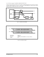
5-1-4-4. PERIPHERAL CIRCUIT
As to the power of lamp, light source of the scanner module, +11.75V(while scanning) supply and +5V(while
waiting) supply are switched by transistor Q7,8,9, and 11.
-Vref is supplied with 1.5V by resistance division through OP-Amp, while +Vref detects the peak by control
of analog Mux U2 during white reference label shading. It detects the peak level of image signals by dividing
shad-on signal and /Shad-rst signal of U2 into High, setting it as top standard voltage. When you scan some
image actually, it will drive shad-on signals into Low to keep the peak level of the capacitor. When you finish
scanning, it will drive /Shad-rst into Low and discharge electricity.
Image signals from CCD mounted on scan PBA in the shuttle scanner are delivered through FPC cable, shift-
ing the level as much as 0.75V at Emitter terminal of Tr which is turned on by Level SH signal. These image
signals will double by an non-inverting amplifier and finally 1.5V level-shifted image signals will be put in
CIP1A.
Содержание SF-4300C
Страница 2: ...ELECTRONICS ...