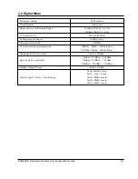

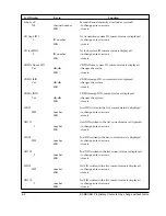

2-3
SAMSUNG Proprietary-Contents may change without notice
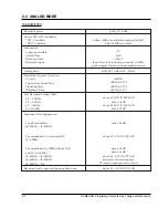
2-3 ANALOG MODE
TRANSMITTER
RF output power
Carrier ON/OFF conditions
ÒONÓ Condition
ÒOFFÓ Condition
Compressor
Compression Rate
Attack Time
Recovery Time
Reference Input
Preamphasis
Maximum Freqency Deviation
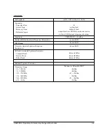
F3 of G3
Supervisory Audio Tone
Signaling Tone
Wideband Data
Post Deviation Limiter Filter
3.0 ~ 5.9KHz
5.9 ~ 6.1KHz
6.1 ~ 15KHz
Over 15KHz
Spectrum Noise Suppression
For all modulation
f0+20KHz ~ f0+45KHz
For modulation by voice and SAT
f0 +45KHz
For modulation by WBD(without SAT)
and ST (with SAT)
f0+45KHz ~ f0+60KHz
f0+60KHz ~ f0+90KHz
f0+90KHz ~ 2f0
Harmonic and conducted Spurious Emissions
0.6W (+2/-4dB)
within ±3dB of specification output (in 2mS)
below-60dBm (in 2mS)
2:1
3mS
13.5mS
Input level for producing a nominal ±2.9KHz
peak freqency deviation of transmitted carrier
6dB/OCT within 0.3 ~ 3KHz
±12KHz
±2KHz (±10%)
±8KHz (±10%)
±8KHz (±10%)
above 40 LOG (F/3000) dB
above 35 dB
above 40 LOG (F/3000) dB
above 28 dB
above 26 dB
above 63 +10 LOG (PY) dB
above 45 dB
above 65 dB
above 63 +10 LOG (PY) dB
(where f0=carrier frequency
PY=mean output power in watts)
below 43 + 10 LOG (PY) dB
Содержание SCH-811
Страница 2: ...Samsung Electronics Co Ltd GH68 00398A 1999 3 REV 1 0 ELECTRONICS ...
Страница 45: ...SAMSUNG Proprietary Contents may change without notice 7 5 7 5 Hands free Kit 1 Exploded View 1 2 3 4 5 6 7 ...
Страница 47: ...SAMSUNG Proprietary Contents may change without notice 7 7 7 7 Speaker Exploded View 1 6 8 9 7 2 5 3 4 ...
Страница 51: ...SAMSUNG Proprietary Contents may change without notice 7 11 7 11 Main packing Exploded View 1 2 8 5 4 7 6 3 ...
Страница 84: ...9 1 Cellular Phone 9 1 1 Main PCB LOGIC B D 9 PCB Diagrams ...
Страница 85: ...9 1 Cellular Phone 9 1 2 Main PCB LOGIC B D ...
Страница 86: ...9 1 Cellular Phone 9 1 3 Main PCB RF B D ...
Страница 87: ...9 1 4 LCD FPC ...
Страница 88: ...9 2 Desk Top rapid Charger PCB Top View ...
Страница 89: ...Bottom View ...
Страница 90: ...9 3 Hands Free kit 1 PCB Top View ...
Страница 91: ...Bottom View ...
Страница 92: ...9 4 Cradle 1 PCB Top View ...
Страница 93: ...9 5 TC PCB Top View Bottom View ...
Страница 94: ...9 6 CLC PCB Top View Bottom View ...
Страница 98: ...10 4 Travel Charger Block Diagram ...
Страница 102: ...10 5 Main Circuit Diagram 1 3 ...
Страница 103: ...Main Circuit Diagram 2 3 ...
Страница 104: ...Main Circuit Diagram 3 3 ...
Страница 105: ...LCD FPC Circuit Diagram ...
Страница 106: ...10 7 Hands Free kit 1 Circuit Diagram data ...
Страница 107: ...Hands Free kit 1 Circuit Diagram audio ...
Страница 108: ...Car Adaptor 1 Circuit Diagram ...
Страница 109: ...10 8 Cradle 1 Circuit Diagram ...
Страница 110: ...10 9 Travel Charger Circuit Diagram ...
Страница 111: ...10 10 CLC Cigarette Lighter Charger Circuit Diagram ...


