Samsung Electronics
5-18
Alignment and Adjustment
5-2-2 Camera System Adjustment
Note :
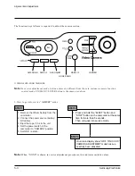
From now on, the structure of every adjustment is as follows.
1. Focus to zoom tracking
Notes :
To maintain proper focus throughout the zoom range, the focus lens position must be changed as
the zoom lens is moved.
During this adjustment the microprocessor will measure the focus positioning requirements at the
wide and telephoto position of the zoom lens.
1) Camera “E-E”.
2) Focus chart (Attached on the last page of this manual).
3) Aim the camera at the focus chart placed 3 meters away and perpendicular to the center of the lens.
The chart should be placed on the flat, gray or white wall.
4) Connect monitor TV jack to video output jack.
5) Press the “DATE/TIME (MODE UP)” and “TITLE(MODE DOWN)” button, so that the OSD start is
“0DE. 3M LEN XX XX”.
6) Press “MENU/ENTER(CONFIRM)” button.
The camera will move both zoom and focus lens. Be sure to do not tremble the lens.
The adjustment is finished when the O.K! message appears on the TV screen.
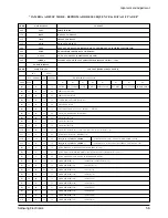
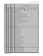
At the wide zoom position, the brightness of picture depends on data of Addr. 0C9, if the picture is dark,
decrease the data of Addr. 0C9.
Step Adjustment Item
1) Mode and input signal/
alignment tape
2) Test point and ADJ. part
3) And after Result and Remarks
Note :
The on-screen display information.
“XX XX” means arbitrary value.
It can be different number depend on the conditions.
ODF T.INI XX XX
(3M
±
1cm)
(Be sure to maintain the distance.)
LENS
CCD
Содержание SCA30
Страница 99: ...Samsung Electronics 8 2 PCB Diagrams 8 1 Main PCB Component Side 8 PCB Diagrams 3 27 95 10 02 AM Page 2 ...
Страница 101: ...Samsung Electronics 8 4 PCB Diagrams 8 2 Main PCB Conductor Side 8 PCB Diagrams 3 27 95 10 02 AM Page 4 ...
Страница 103: ...Samsung Electronics 8 6 PCB Diagrams 8 3 Main PCB Hi 8 Component Side 8 PCB Diagrams 3 27 95 10 02 AM Page 6 ...
Страница 104: ...Samsung Electronics 8 7 PCB Diagrams 8 PCB Diagrams 3 27 95 10 02 AM Page 7 ...
Страница 105: ...Samsung Electronics 8 8 PCB Diagrams 8 4 Main PCB Hi 8 Conductor Side 8 PCB Diagrams 3 27 95 10 02 AM Page 8 ...
Страница 106: ...Samsung Electronics 8 9 PCB Diagrams 8 PCB Diagrams 3 27 95 10 02 AM Page 9 ...
Страница 111: ...Samsung Electronics 8 14 PCB Diagrams 8 9 CVF PCB Component Side Conductor Side 8 PCB Diagrams 3 27 95 10 03 AM Page 14 ...
Страница 113: ...Samsung Electronics 8 16 PCB Diagrams 8 11 CCD PCB 8 12 Function PCB 8 PCB Diagrams 3 27 95 10 03 AM Page 16 ...
Страница 116: ...Samsung Electronics 10 2 Schematic Diagrams 10 1 DC DC Converter Main 10 Schematic Diagrams 3 27 95 10 04 AM Page 2 ...
Страница 118: ...Samsung Electronics 10 4 Schematic Diagrams 10 3 Video Normal Main 10 Schematic Diagrams 3 27 95 10 04 AM Page 4 ...
Страница 119: ...Samsung Electronics 10 5 Schematic Diagrams 10 4 Video Hi 8 Main 10 Schematic Diagrams 3 27 95 10 04 AM Page 5 ...
Страница 120: ...Samsung Electronics 10 6 Schematic Diagrams 10 5 Audio Mono Main 10 Schematic Diagrams 3 27 95 10 04 AM Page 6 ...
Страница 121: ...Samsung Electronics 10 7 Schematic Diagrams 10 6 Audio Stereo Main 10 Schematic Diagrams 3 27 95 10 04 AM Page 7 ...
Страница 122: ...Samsung Electronics 10 8 Schematic Diagrams 10 7 Camera Main 10 Schematic Diagrams 3 27 95 10 04 AM Page 8 ...
Страница 123: ...Samsung Electronics 10 9 Schematic Diagrams 10 8 Rear 10 Schematic Diagrams 3 27 95 10 04 AM Page 9 ...
Страница 124: ...Samsung Electronics 10 10 Schematic Diagrams 10 9 CCD 10 Schematic Diagrams 3 27 95 10 04 AM Page 10 ...
Страница 125: ...Samsung Electronics 10 11 Schematic Diagrams 10 10 CVF 10 Schematic Diagrams 3 27 95 10 04 AM Page 11 ...
Страница 126: ...Samsung Electronics 10 12 Schematic Diagrams 10 11 EVF 10 Schematic Diagrams 3 27 95 10 04 AM Page 12 ...
Страница 127: ...Samsung Electronics 10 13 Schematic Diagrams 10 12 Front with EIS 10 Schematic Diagrams 3 27 95 10 04 AM Page 13 ...
Страница 130: ...Samsung Electronics 10 16 Schematic Diagrams 10 15 FUNCTION 10 Schematic Diagrams 3 27 95 10 04 AM Page 16 ...


