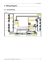
Samsung PS60F5500AWXXH Скачать руководство пользователя страница 58

5. Wiring Diagram

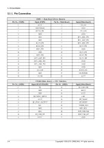
5.1.1. Pin Connection

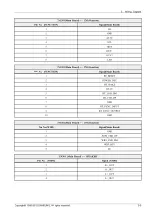
SMPS ↔ Main Board [Power Harness]

Pin No. (SMPS)

Signal (SMPS)

Pin No. (Main Board)

Signal (Main Board)

1

A5.3V

1

VS_ON

2

SW-POWER

2

GND

3

B15VS_PW

3

VS_CON

4

GND

4

GND

5

GND

5

B5V_ASIC_PW

6

GND

6

B5V_ASIC_PW

7

B5.3V_PW

7

B5V_ASIC_PW

8

B5.3V_PW

8

B15V_PW

9

B15V_PW

9

GND

10

GND

10

B15V_PW

11

B15V_PW

11

B5.3V_PW

12

B5V_ASIC_PW

12

B5.3V_PW

13

B5V_ASIC_PW

13

GND

14

B5V_ASIC_PW

14

GND

15

GND

15

GND

16

VS_CON

16

B15VS_PW

17

GND

17

SW-POWER

18

VS_ON

18

A5.3V

CN1202 (Main Board) ↔ CN1 (Function)

Pin No. (SMPS)

Signal (MAIN BOARD)

Pin No. (SMPS)

Signal (Main Board)

1

IR

12

BT_USB_DM

2

GND

13

KEY2

3

GND

14

B5.2V

4

BT_SYNC_INPUT

15

LED

5

A3.3V

16

BT_WAKE

6

BT_SYNC_OUTPUT

17

BT_RESET

7

SCL

18

POWER_DET

8

GND

19

WIFI_B5V

9

SDA

20

WIFI_USB_DM

10

BT_USB_DP

21

WIFI_USB_DP

11

KEY1

22

GND

5-4

Copyright© 1995-2013 SAMSUNG. All rights reserved.

Содержание PS60F5500AWXXH

Страница 1: ...0F5500AWXXH SERVICEMANUAL Plasma TV PS60F5500AW Contents 1 Precaution 2 Product Specification 3 Disassembly and Reassembly 4 Troubleshooting 5 Wiring Diagram Refer to the service manual in the GSPN se...

Страница 2: ...ooting 4 1 4 1 First Checklist for Troubleshooting 4 1 4 2 Checkpoints by Error Mode 4 2 4 2 1 Example of Trouble Shooting 4 7 4 2 2 Operating Logic LED 4 9 4 3 Factory Mode Adjustments 4 11 4 3 1 Det...

Страница 3: ...REN T TESTER TES T ALL EXPOSED ME TAL SUR FACES 2 WIRE CORD ALSO TES T WITH PLUG REVERSED USING AC ADAPTER PLUG AS REQU IRED EARTH GROUND R E A D I N G SHOULD NOT BE ABOVE 0 5mA Figure 1 1 AC Leakage...

Страница 4: ...if the wiring is too tight incorrectly placed or loose Never change the space between the part and the printed circuit board Check the AC power cord for possible damages Keep the part or the lead away...

Страница 5: ...lade of the AC plug and that of any conductive materials i e the metal panel input terminal earphone jack etc 6 Insulation Check Process Unplug the power cord from the AC source and turn the switch on...

Страница 6: ...for soldering purposes 6 Use only anti static solder removal devices Most solder removal devices do not support an anti static feature A solder removal device without an anti static feature can store...

Страница 7: ...antenna cable or the external connectors if they are fully unplugged Damage to the cord may cause fire or electric shock 6 Keep the antenna far away from any high voltage cables and install it firmly...

Страница 8: ...Without Stand 1396 9 x 57 0 x 831 3 60 With Stand 1396 9 x 375 5 x 928 Without Stand 1483 8 x 57 0 x 877 1 Dimensions W x D x H inch 64 With Stand 1483 8 x 375 5 x 974 5 Without Stand 18 5 kg 51 With...

Страница 9: ...0 C 10 to 80 non condensing 4 F to 113 F 20 C to 45 C 5 to 95 non condensing Stand Swivel Left Right 20 20 Dimensions W x H x D Body 46 9 x 27 9 x 2 2 inches 1191 9 x 709 1 x 57 0 mm 54 9 x 32 7 x 2 2...

Страница 10: ...er Canceller X X Wide Color Enhancer Plus O O Film Mode O O Picture Relax Mode Support X X Dolby Dolby Digital Plus Pulse Dolby Digital Plus Pulse SRS DNSe DTS Studio Sound SRS Theater Sound HD dts 2...

Страница 11: ...3 Power Cord 3903 000551 Batteries AAA x 2 4301 000103 TV MIC STB SOUR CE VOICE MORE VOL CH LIGHT DVR MENU 3D SMART HUB GUIDE RETURN EXIT Remote Control AA59 00773A Stand Wire Holder BN61 08370A Clean...

Страница 12: ...nents 3 1 Overall Disassembly and Reassembly CAUTION Disconnect the PDP TV from the power source before disassembly Follow these directions carefully never use metal instruments to pry apart the cabin...

Страница 13: ...Description Description Photo Screw 60 60 6003 001782 M4 L12 2 Remove the screws of rear cover 51 6003 001782 M4 L12 6003 000337 M4 L10 60 6003 001782 M4 L12 6003 000337 M4 L10 Copyright 1995 2013 SAM...

Страница 14: ...remove the rear cover 51 60 4 Remove the screws of main board CAUTION Disconnect all connectors prior to removing boards 6001 002606 M3 L10 5 Remove the screws of SMPS Remove the SMPS 51 60 6001 00260...

Страница 15: ...on 6001 002606 M3 L10 Remove the screw of WI FI module Remove the WI FI module WI FI code BN59 01161A 6001 002606 M3 L10 Remove the screw of blue tooth module Remove the blue tooth module Blue tooth c...

Страница 16: ...ption Description Photo Screw Remove the screw of Cover bottom 6003 001782 M4 L12 6003 000337 M4 L10 8 Remove the screws of the front cover 51 6003 001782 M4 L12 60 6003 001782 M4 L12 3 5 Copyright 19...

Страница 17: ...e problem is caused by Main board or Logic Board No Video If the problem is No Video but Logic Board is on and Indication LED is blinking repeatedly and faster than normal booting replace the Logic bo...

Страница 18: ...r the LEDs on the front panel does not work when connecting the power cord if the cables are improperly connected or the Main Board or SMPS is not functioning In this case check the following Check th...

Страница 19: ...N101 connector Are the SMPS CN4007 and Main CN201 connected Replace Fuse F801S Is the Fuse F801S of the SMPS Power Input Part Open Replace the SMPS SMPS CN801 PIN2 STB 5V PIN1_PS ON Check to see if it...

Страница 20: ...ayed on the screen Major Checklist The output voltage of the Main SMPS This may happen when the LVDS cable connecting the Main Board and the Panel is disconnected Diagnostics Module FFC Cable 51 PDP M...

Страница 21: ...y Replace the SMPS Check All output voltages on SMPS Are all voltage nermal Check the LED operation of Logic Board whitch is normally operating Normal Blink once a second No No No Check Replace the X...

Страница 22: ...Cable CN801 51 60 PDP Yes Yes Yes Replace the Speaker Replace the SMPS Is the output voltage of SMPS normal CN801 PIN 7 15V Replace the Main board 1 Is the speaker output terminal of the Main board n...

Страница 23: ...screen appears when the TV is turned on The Scale is not resecting Replace the Main board The OSD box appears but there is no text Incorrect program version Check the version of each program Replace...

Страница 24: ...rs on the screen The SMPS voltage is incorrect Adjust the SMPS voltage according to the voltage printed on the module label Dim screen blurred in red X Main board defect Replace the X Main board A bla...

Страница 25: ...4 Troubleshooting 4 2 2 Operating Logic LED Normal LED blink time is once per 0 5s Abnormal LED Blink interver is 0 3s and Off time 4s Copyright 1995 2013 SAMSUNG All rights reserved 4 9...

Страница 26: ...4 Troubleshooting PDP Module Action 4 10 Copyright 1995 2013 SAMSUNG All rights reserved...

Страница 27: ...PN51F5500 PN60F5500 Vendor SDI SDI Code BN96 25240A BN96 25241A Panel Spec SMPS Code BN44 00600A BN94 06194B Chassis Ass y BN94 06194A BN91 10288B Main Assy PBA Ass y code BN97 07107W BN97 07107X Fac...

Страница 28: ...ctory Mode To enter Service Mode Press the remote control keys in this sequence If you do not have Factory remote control o o o o o o If you have Factory remote control INFO Factory 4 12 Copyright 199...

Страница 29: ...S232C OFF SDAL X12 MAIN xxxx xxxx RFS X12 0071 KER 201x xx xx KERNEL 8 0837 D Onboot xxxx x Backend IC x Data Ver xxxx TCON Version xxxx DTP DTVTD xxxx Model PN51F5500 Wired MAC SUCCESS Wireless MAC S...

Страница 30: ...nP Language ENG_US WIFI REGION S OTN Support ON OTA Support OFF TTX OFF China HD OFF NT Conversion OFF Num of DTV 1 Num of AV 1 Num of COMP 1 Num of HDMI 3 Num of SCART 0 Num of USB Port 2 Num of Head...

Страница 31: ...upport ON BT Support ON BT ADDRESS Engineer Option Auto Power MEMORY Type Of PANEL KEY None 5 Way Function Key L_BACK Contents Bar OFF Cable Modulation QAM Standby led on off OFF Recognition Support I...

Страница 32: ...ype development Info Link Country None TTX Group Visual Test MediaPlayDB OPTION_SWU OTN Server Type operating OTN Test Server OFF SWU Reset SWU Duration OFF SWU Fail Test OFF OPTION_NUM Num of ATV 1 N...

Страница 33: ...Temperature 0 LOGIC Waveform Day 0 Logic CheckSum 0 MRT 0 SAPC Timer APC Speed Hotel Option Hospitality Mode OFF Power On Menu OSD Operation Music Mode External Source Eco Solution Cloning Shop Optio...

Страница 34: ...ow THID 3 Carrier2 SNR High THR 16 Carrier2 SNR Low THR 80 Sig Error On 35 Sig Error Off 41 Amp Model TAS5745 Amp Volume 0xcbh Amp Scale 0x2Fh Amp Check Sum Woofer Type 0 Woofer Scale 0x8ah Woofer Che...

Страница 35: ...ON OFF ON FRC LVDS SSC MRR 10 FRC LVDS SSC MFR 1 FRC LVDS SSC Period 1 FRC LVDS SSC Modulation 1 FRC DDR SSC ON OFF ON FRC DDR SSC MRR 15 FRC DDR SSC MFR 1 FRC DDR SSC Period 1 Spread Spectrum FRC DDR...

Страница 36: ...deldy 15 TCON_TEMP READ 1 TEMP LAST 1 DCC VERSION 1 DCC CHK SEL 0 DCC CHECK LOCAL 0x0 DCC CHECK TOTAL 0x0 MulitACC Checksum 0 FRC IIC Bus stop OFF DVB SNR BER Signal Strength Bandwidth Frequency LNA S...

Страница 37: ...1 IF AGC_1 TMCC Lock_1 TS Packer_1 Master Lock_1 A_Modulation_1 A_Code Rate_1 A_Timer InterLeave_1 A_Segments Num_1 A_BER_1 B_Modulation_1 B_Code Rate_1 B_Timer InterLeave_1 B_Segments Num_1 B_BER_1 C...

Страница 38: ...WB Pattern OFF HDMI Pattern Sel 0 Parma Pre Test Pattern 0 Test Pattern Parma Post Test Pattern 0 Panel Display Time 0Hr SVC Info 0 Delete S N 0 T CON Usb Download T CON CheckSum Logic Usb D L Failut...

Страница 39: ...ew 0 Delete Log Debug Log Down LOG View Log Emergency Log Copy Loop Back LAN Test AV Audio Test DVIN Audio Test CVBS Test COMP Test USB HUB Test HDMI Test SCART Audio Test SCART CVBS Test SCART RGB Te...

Страница 40: ...ensor BT EXT Sound Inspection Woofer Sound Inspection NONE ATV CH Inspection DTV CH Inspection Satellite CH Inspection IPERF Stopped OPTION HDMI Expert DVB CI CAL Data Backup CAL Data Restore 4 24 Cop...

Страница 41: ...d_G_L 132 2nd_B_L 132 2nd_R_H 70 2nd_G_H 70 ADC Result 2nd_B_H 70 R Offset 128 G Offset 128 B Offset 128 R Gain 128 G Gain 128 B Gain 128 WB_W2_R_Offset 128 WB_W2_B_Offset 128 WB_W2_R_Gain 164 WB_W2_B...

Страница 42: ...ark G3_Gain R4_Gain B4_Gain G4_Gain R5_Gain B5_Gain G5_Gain R6_Gain B6_Gain G6_Gain R7_Gain B7_Gain G7_Gain R8_Gain B8_Gain G8_Gain R9_Gain B9_Gain G9_Gain R10_Gain B10_Gain G10_Gain 4 26 Copyright 19...

Страница 43: ...4 Troubleshooting 4 4 White Balance Calibration Copyright 1995 2013 SAMSUNG All rights reserved 4 27...

Страница 44: ...z 3 Pattern Pattern 24 Chess Pattern 4 Use Equipment CA210 Master MSPG925 Generator Use other equipment only after comparing The result with that of The Master equipment Input mode Calibration Pattern...

Страница 45: ...onent1 mode 3 Enter Service mode 4 Select the ADC menu 5 Select the Comp Calibration menu 6 In Comp Calibration Off status press the key to perform Calibration 7 When Calibration is complete it return...

Страница 46: ...oting 4 4 3 White Balance Adjustment ADC WB White Balance Factory Low light High light Sub Bright R offset G offset B offset Sub Contrast R gain G gain B gain 4 30 Copyright 1995 2013 SAMSUNG All righ...

Страница 47: ...are version after the upgrades are complete the new version will have a higher number than the older version When software is upgraded video and audio settings you have made will return to their defau...

Страница 48: ...1 0x01 0x00 AV2 0x01 AV AV3 0x02 S Video1 0x02 0x00 S Video2 0x01 S Video S Video3 0x02 Component1 0x03 0x00 Component2 0x01 Component Component3 0x02 PC1 0x04 0x00 PC2 0x01 PC PC3 0x02 HDMI1 0x05 0x0...

Страница 49: ...0x02 RGB Only Mode Blue 0x03 Auto 0x06 0x00 Native 0x01 Color Space Custom 0x02 White Balance R Offset LCD 0x07 0 50 White Balance G Offset LCD 0x08 0 50 White Balance B Offset LCD 0x09 0 50 White Bal...

Страница 50: ...Level Low 0x01 Off 0x05 0x00 Auto1 0x01 Film Mode Auto2 0x02 Off 0x06 0x00 Clear 0x01 Standard 0x02 Smooth 0x03 Custom 0x04 Picture Option Auto Motion Plus Demo 0x05 16 9 0x0b 0x0a 0x01 0x00 Zoom1 0x0...

Страница 51: ...x04 Balance 0x01 0x00 0 20 100hz 0x01 0 20 300hz 0x02 0 20 1khz 0x03 0 20 3khz 0x04 0 20 10khz 0x05 0 20 Equalizer Reset 0x06 0x00 SRS TruSurround HD Genoa Off 0x02 0x00 0x00 Virtual Surrond X6 On 0x0...

Страница 52: ...Select Sub 0x01 Sound Reset Sound Reset 0x09 0x00 0x00 KEY Key Generation 0x0d 0x00 0x00 refer to the table of below Key value Value Up 96 0x60 Down 97 0x61 Left 101 0x65 Right 98 0x62 Menu 26 0x1A In...

Страница 53: ...4 Troubleshooting 4 7 Rear Cover Dimension PF5500 51 COVER REAR Dimension PF5500 60 COVER REAR Dimension Copyright 1995 2013 SAMSUNG All rights reserved 4 37...

Страница 54: ...2 1 702 1 634 5 26 3 41 3 671 0 PF5500 60 1388 3 1333 5 924 1 823 3 754 4 27 5 41 3 819 0 Model Inch I J K L M N O P PF5500 51 55 7 307 2 400 0 400 0 496 9 891 5 36 4 79 5 PF5500 60 55 7 375 5 600 0 4...

Страница 55: ...CN5502 CN5503 CN5504 CN5505 CN5506 CN2501 CN2012_LO CN2013_LO CN4002 CN4002 CN2601 CN201 CN801 CN2010_LO CN1201 Y Buffer SMPS Logic Main Board E BUFFER CN1 FUNCTION E BUFFER Speaker L Speaker R CN301...

Страница 56: ...2 CN4002 CN2609 CN201 CN801 CN2010_LO CN1201 SMPS Logic Main Board E BUFFER CN1 FUNCTION E BUFFER Speaker L Speaker R CN301 CN5000 CN4003 CN5008 CN5005 CN5004 CN5009 CN2011_LO Y Buffer X Buffer NOTE T...

Страница 57: ...g Diagram 51 Cable Lead connector Use POWER 18 Pin Code 51 BN39 01781A 130mm Photo 60 Cable Lead connector Use POWER 18 Pin Code 60 BN39 01781B 150mm Photo Copyright 1995 2013 SAMSUNG All rights reser...

Страница 58: ...PW 11 B5 3V_PW 12 B5V_ASIC_PW 12 B5 3V_PW 13 B5V_ASIC_PW 13 GND 14 B5V_ASIC_PW 14 GND 15 GND 15 GND 16 VS_CON 16 B15VS_PW 17 GND 17 SW POWER 18 VS_ON 18 A5 3V CN1202 Main Board CN1 Function Pin No SMP...

Страница 59: ...N Signal Main Board 1 BT_RESET 2 POWER_DET 3 BT_WAKE 4 B5 2V 5 BT_USB_DM 6 BT_USB_DP 7 GND 8 BT_SYNC_INPUT 9 BT_SYNC_OUTPUT 10 GND CN1201 Main Board CN1 Function Pin No WIFI Signal Main Board 1 GND 2...

Страница 60: ...a Japan https gspn2 samsungcsportal com N America S America https gspn3 samsungcsportal com This Service Manual is a property of Samsung Electronics Co Ltd Any unauthorized use of Manual can be punish...

Отзывы: