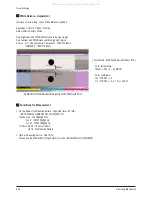
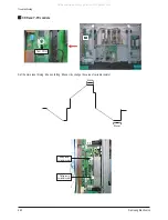
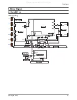
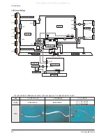
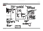
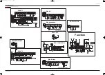
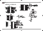

Wiring Diagram
6-4
Samsung Electronics
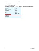
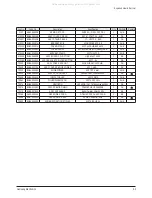
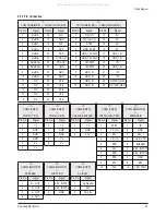
42" Loc. No.
50" Loc. No.
Description
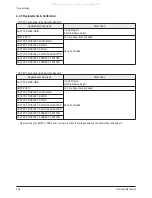
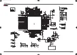
CN5401
CN5401
Horizontal Y-scan line(1~128) of Module and Y-Main Scan Connect
CN5402
CN5402
Horizontal Y-scan line(129~256) of Module and Y-Main Scan Connect
CN5403
CN5403
Horizontal Y-scan line(256~384) of Module and Y-Main Scan Connect
-
CN5512
Y-Main Scan(High) and Y-Main Scan(Low) Connect
CN5501
CN5501
Horizontal Y-scan line(384~512) of Module and Y-Main Scan Connect
CN5502
CN5502
Horizontal Y-scan line(512~640) of Module and Y-Main Scan Connect
CN5503
CN5503
Horizontal Y-scan line(640~768) of Module and Y-Main Scan Connect
CN5407
CN5407
Upper Y-Drive and Y-Main Scan Connect
CN5507
CN5507
Lower Y-Drive and Y-Main Scan Connect
CN5707
CN5707
Vs(205V),Vg(15v) Power input connect(6Pin) of Y-Drive
CN5701
CN5701
Y-Drive control signal from Logic Board
CN810
CN810
Vs(205V),Vg(15v) Power input connect(6Pin) of SMPS for Y-Drive
CN809
CN809
Vs(205V),Vg(15v) Power input connect(6Pin) of SMPS for X-Drive
CN808
CN808
Va(63V) ,5.3V Power input connect(3Pin) of SMPS for F-Buffer
CN807
CN807
Power input connect(10pin) for Logic Board
CN801
CN801
Image signal(LVDS) connect(41pin) from Main Board
CN800
CN800
AC Power input connect from AC-inlet
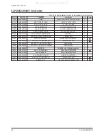
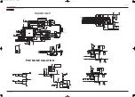
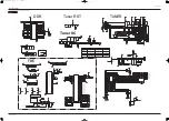
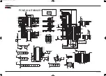
CN4002
CN4002
Horizontal X-scan line of Module and X-scan Connect(first Block)
CN4001
CN4001
Horizontal X-scan line of Module and X-scan Connect(second Block)
-
CN4000
Horizontal X-scan line of Module and X-scan Connect(third Block)
CN2000
CN2000
Power input connect(10pin) of Logic Board from SMPS
CN2001
CN2001
Image signal(LVDS) connect(41pin) of Logic board from Main Board
CN2002
CN2002
Y-Drive control signal of Logic Board
CN2004
CN2005
Address Data(684th~1366th) connect for F-Buffer board
CN2028
CN2004
Address Data(1st~683th) connect for E-Buffer board
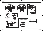
CN2500
CN2500
Address Data(1st~683th) connect from Logic Board
CN2510
CN2510
Power input connect from F-Buffer Board
CN2610
CN2610
Power input connect to E-Buffer Board
CN2600
CN2600
Address Data(684th~1366th) connect from Logic board
CN2609
CN2609
Va(63V) ,5.3V Power input connect(3Pin) from SMPS
CN1101
CN1101
Power input connect(24Pin) from SMPS
CN2202_HD
CN2202_HD
Image signal(LVDS) connect(30pin) for Logic board
CN1605_PDP
CN1605_PDP
Function input(source,ch up/down...) connect on Main board
CN1606
CN1606
Power SW input connect on Main Board
CN1203
CN1203
Speak out connect on Main Board
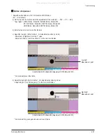
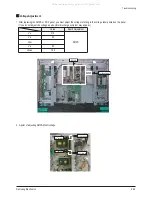
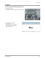
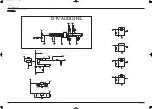
6-1-2 Connector role
All manuals and user guides at all-guides.com
Содержание PS50C62HX
Страница 9: ...1 6 Samsung Electronics MEMO All manuals and user guides at all guides com...
Страница 13: ...2 4 Samsung Electronics MEMO All manuals and user guides at all guides com...
Страница 25: ...3 12 Samsung Electronics MEMO All manuals and user guides at all guides com...
Страница 58: ...MEMO Samsung Electronics 4 33 All manuals and user guides at all guides com...
Страница 67: ...7 2 Samsung Electronics MEMO All manuals and user guides at all guides com...


