


1-2
Samsung Electronics
Precaution
6. Components, parts and wiring that appear to have overheated or that are otherwise damaged should be
replaced with parts that meet the original specifications. Always determine the cause of damage or overheating,
and correct any potential hazards
7. Observe the original lead dress, especially near the following areas: Antenna wiring, sharp edges, and
especially the AC and high voltage power supplies. Always inspect for pinched, out-of-place, or frayed wiring.
Do not change the spacing between components and the printed circuit board. Check the AC power cord for
damage. Make sure that no wires or components touch thermally hot parts.
8. Product Safety Notice:
Some electrical and mechanical parts have special safety-related characteristics which might not be obvious
from visual inspection. These safety features and the protection they give might be lost if the replacement
component differs from the original--even if the replacement is rated for higher voltage, wattage, etc.
9. Components that are critical for safety are indicated in the circuit diagram by shading, or . Use
replacement components that have the same ratings, especially for flame resistance and dielectric strength
specifications. A replacement part that does not have the same safety characteristics as the original might
create shock, fire or other hazards.
Содержание HT-C553
Страница 8: ...3 4 Samsung Electronics MEMO...
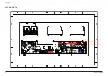
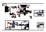
Страница 23: ...6 2 Samsung Electronics PCB Diagram 6 2 FRONT PCB Top FCON1 UIC2 KIC2 U1 2 1...
Страница 25: ...6 4 Samsung Electronics PCB Diagram 6 3 FRONT PCB Bottom...
Страница 26: ...Samsung Electronics 6 5 PCB Diagram 6 4 KEY PCB Top...
Страница 27: ...6 6 Samsung Electronics PCB Diagram 6 5 KEY PCB Bottom CN1 IC1 1...
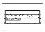
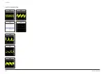
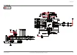
Страница 31: ...6 10 Samsung Electronics PCB Diagram TP1 TP2 TP3 TP4 TP5 6 6 2 Test Point Wave Form TP6 TP7...
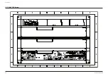
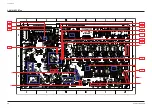
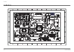
Страница 32: ...Samsung Electronics 6 11 PCB Diagram 6 7 MAIN PCB Bottom IC2 IC20 IC35 IC16 IC3 IC8 IC1 AIC22 AIC16...
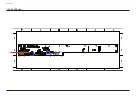
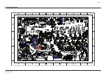
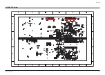
Страница 33: ...6 12 Samsung Electronics PCB Diagram 6 8 SMPS PCB Top CON1...
Страница 34: ...Samsung Electronics 6 13 PCB Diagram 6 9 SMPS PCB Bottom CON2 CON3...
Страница 35: ...6 14 Samsung Electronics MEMO...
Страница 47: ...2 8 Samsung Electronics MEMO...
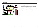
Страница 68: ...Samsung Electronics 4 9 Troubleshooting AV I O page 7 7 IC10 IC11 IC36 MAIN PCB Top page 6 8 Fig 4 6 2 2 2...
Страница 72: ...Samsung Electronics 4 13 Troubleshooting AV I O page 7 7 IC11 IC36 MAIN PCB Top page 6 8 Fig 4 9 4 5 4 5 4 5...
Страница 73: ...4 14 Samsung Electronics Troubleshooting AV I O page 7 7 IC11 IC36 MAIN PCB Top page 6 8 Fig 4 10 6 6 6...


