Alignment and Adjustments
Samsung Electronics
4-15
4-6 Hige Voltage Part
4-6-1 PWM REG Circuit
For the existing high voltage REG circuit (input
voltage variation type), a dynamic REG response
is not provided. So it is difficult for both beam
linearity and uniformity in screen size to be
maintained on the screen with rapidly changing
beams.
A PWM (Pulse Width Modulation) type of high
voltage, however, provides the maintenance of
beam linearity and uniformity in screen size via a
quick response to beam change by performing
sync lock every 1H line, and detecting beam
fluctuation at 1H line, and then controlling the IC
current of high voltage output circuit.
1. High Voltage Fluctuation Detect (DC Detect)
FBT pin 11 detects DC high voltage fluctuation.
The detected DC high voltage value is input to
PWM IC471 pin1 through R473, VR471, R471,
and then it is input to a differential AMP circuit
that differentiates the gap after comparing with
the reference voltage input to pin2.
2. High Voltage Fluctuation Detect (AC Detect)
To check AC high voltage fluctuation, the
output from FBT is detected by using a
capacitor inside the high voltage distributor. The
detection of AC high voltage fluctuation,
a detection of dynamic beam current change is
required in order to keep beam linearity and
uniformity in size.
Regarding the capacitor, a capacity of less than
3000P should be applied to a PWM type. (The
existing type needs a capacity of about 6000P.)
AC detect circuit eliminates unnecessary high
frequency by using C476, D472. Also, AC gain is
limited to + / - 0.7V (D472). This AC gain is
combined with the detection value of DC high
voltage fluctuation by using C478.
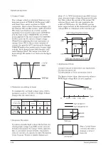
3. PWM IC OSC Sync Lock
A PWM type IC needs sync lock for PWM pulse
and horizontal scan line.
The standard time constant of OSC circuit is
determined by C487, R475 (PWM IC pins 5 and 6).
And the standard OSC frequency is about 27
kHz . The horizontal frequency of scan line is
31.5kHz(NT), 3375kHz(DTV), 15.75kHz(Interface),
so sync lock for this horizontal frequency should
be performed using sync lock circuit. The sync
lock circuit consists of Q481(Tr KSC815-Y),
D479, D478, and C492. The input AFC signal is
connected to PWM IC pin 5 through D479 so
that it can be negative Trig.
4. Dead Time (HV Protect)
Dead Time (PWM IN pin4) consists of C481,
delays high voltage for a certain time to soft
start in power on, a x-ray protection circuit.
The voltage of Dead Time is detected by FBT
pin7 and through DC Feedback. The normal
voltage of Dead Time is +27V. When high
voltage increases, however, detected voltage is
in proportion to high voltage. Then, the detected
voltage is applied to ICR01S(TL431).
If the voltage is over 2.5V (normal:about 2.25V),
TL431 turns ON, the base port of QR401S
becomes low, and then an emitter current flows.
At this time, a high voltage protection point is
set. When QR401S turns ON, high voltage is
applied to PWM IC pin4 and then muted.
OSC : 27KHz
AFC Waveform : 31.5KHz(NT)
Locked OSC Waveform : 31.5KHz
Содержание HCN5527WX/XAA
Страница 9: ...Reference Information 2 4 Samsung Electronics 2 3 IC Line Up 2 3 1 Progressive...
Страница 10: ...Reference Information Samsung Electronics 2 5...
Страница 11: ...Reference Information 2 6 Samsung Electronics 2 4 MICOM IIC BUS LINE UP...
Страница 13: ...MEMO 3 2 Samsung Electronics...
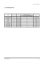
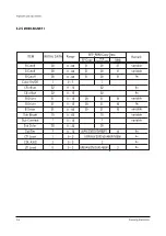
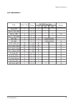
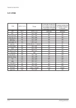
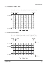
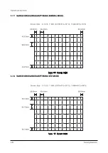
Страница 31: ...Alignment and Adjustments 4 18 Samsung Electronics 4 7 3 473W 4715W NORMAL MODE 4 7 4 473W 4715W DTV MODE...
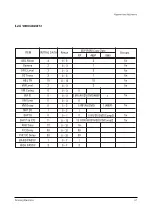
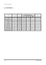
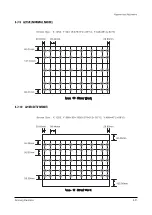
Страница 34: ...Alignment and Adjustments Samsung Electronics 4 21 4 7 9 6215R NORMAL MODE 4 7 10 6215R DTV MODE...
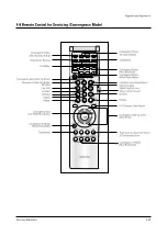
Страница 36: ...Alignment and Adjustments Samsung Electronics 4 23 4 8 Remote Control for Servicing Convergence Mode...
Страница 51: ...MEMO 4 38 Samsung Electronics...
Страница 55: ...MEMO 5 4 Samsung Electronics...
Страница 69: ...7 12 Samsung Electronics MEMO...
Страница 78: ...TP02 TP01 10 Schematic Diagrams Samsung Electronics Schematic Diagrams 10 1 10 1 MAIN 1 TP01 TP02...
Страница 79: ...Schematic Diagrams 10 2 Samsung Electronics TP20 TP03 TP04 10 2 MAIN 2 TP03 TP04 TP20...
Страница 80: ...Samsung Electronics Schematic Diagrams 10 3 10 3 MAIN 3 TP12 TP13 TP12 TP13...
Страница 82: ...Samsung Electronics Schematic Diagrams 10 5 10 5 MICOM...
Страница 83: ...Schematic Diagrams 10 6 Samsung Electronics 10 6 CRT...
Страница 84: ...Samsung Electronics Schematic Diagrams 10 7 10 7 SUB 1 TP21 TP21...
Страница 85: ...Schematic Diagrams 10 8 Samsung Electronics 10 8 SUB 2 TP24 TP23 TP22 TP22 TP23 TP24...
Страница 86: ...Samsung Electronics Schematic Diagrams 10 9 10 9 CONVERGENCE SDC12 1...
Страница 87: ...Schematic Diagrams 10 10 Samsung Electronics 10 10 CONVERGENCE SDC12 2...
Страница 88: ...Samsung Electronics Schematic Diagrams 10 11 10 11 PRO SCAN 1...
Страница 89: ...Schematic Diagrams 10 12 Samsung Electronics 10 12 PRO SCAN 2...
Страница 90: ...Samsung Electronics Schematic Diagrams 10 13 10 13 PRO SCAN 3...
Страница 91: ...Schematic Diagrams 10 14 Samsung Electronics 10 14 PRO SCAN 4...
Страница 92: ...10 15 CG AMP Samsung Electronics Schematic Diagrams 10 15...
Страница 93: ...Schematic Diagrams 10 16 Samsung Electronics 10 16 AV FRONT...
Страница 94: ...10 17 CONTROL Samsung Electronics Schematic Diagrams 10 17...
Страница 95: ...Schematic Diagrams 10 18 Samsung Electronics 10 18 DY JACK SENSOR DY JACK SENSOR...

