


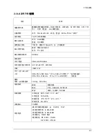


10 Operating Instructions and Installation
10-4
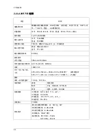
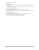
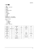
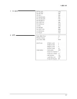
8. Connecting Computer
- Connect the D- Sub cable (optional) to "PC (PC IN)" on the rear of your set and the other end to the Video Card of
your computer.
- Connect the stereo audio cable (optional) to "AUDIO (PC IN)" on the rear of your set and the other end to "Audio
Out" of the sound card on your computer.
9. Connecting External A/V Devices (AV IN 1)
- Connect RCA cable to an appropriate external A/V device such as VCR, DVD or Camcorder.
- Connect RCA audio cables to "R - AUDIO - L" on the rear of your set and the other ends to corresponding audio out
connectors on the A/V device.
10. Connecting External A/V Devices (AV IN 1)
- The Kensington lock (optional) is a device used to physically fix the system when used in a public place.
- If you want to use a locking device, contact the dealer where you purchased the TV.
- The place of the Kensington Lock may be different depending on its model.
Содержание GBD26KS
Страница 2: ... 豪华超薄设计 超级画质 超级音质 极其舒适 使用方便 ...
Страница 7: ...Memo 1 Precautions 1 4 ...
Страница 11: ... _ _ _ _ ab ab ab ab c c c c IJ Id MN U ...
Страница 13: ... uvZwæïxyz 9 0 óô b 2 9 3 bcd ÌÍ 6 ÌÍ d 5 053 Ò Ô Ñ Þ qt 6 d 4 4 4 Ò 4 4 4 4 Þ 4 qt ª 5 _ gbB ÎÏ_ ...
Страница 22: ... ...
Страница 23: ... 0 1234453 6789 AB CDEF GHIJ GK GK GK GK GLCM 1NOPQ RSTUV WXYZ LC YZ 23 _ ...
Страница 27: ... F F F F º D D D D wx ny gh t t t I 0 9 0 9 B EF EF CDEF 4 4 PQ PQ PQ PQ L ...
Страница 28: ... L L 6 À Á cd 8 8 8 à 8 8 8 ...
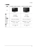
Страница 30: ...10 2 Connection Panel 10 Operating Instructions and Installation 10 2 ...
Страница 35: ... 0123 45 6789 ABCDEFGHI JIK LM N O PQR LST O PQR ...
Страница 36: ... UVMNW OST LSTXY OQR WUVSTXY ...
Страница 37: ... LZI O LZI OQR WUVZI ...
Страница 38: ... L OQR LAZXY OQR UVAZXY ...
Страница 39: ... UV _AZ ab ...
Страница 40: ... ...
Страница 44: ... ...
Страница 45: ... ...
Страница 46: ... ...
Страница 47: ... ...
Страница 48: ... ...
Страница 51: ... g Þ Õ Ì W L N0 õö k kü ...
Страница 52: ... y UV e J V y h e G y UV h e ...
Страница 55: ...13 Circuit Descriptions 13 3 13 2 Main Block ...
Страница 56: ...13 Circuit Descriptions 13 4 13 3 SMPS Board 13 3 1 26 32 SMPS Block 13 3 2 26 32 SMPS Block ...
Страница 57: ...13 Circuit Descriptions 13 5 13 3 3 26 32 SMPS Block 13 3 4 26 32 SMPS Block ...
Страница 58: ...13 Circuit Descriptions 13 6 ...
Страница 59: ...13 Circuit Descriptions 13 7 13 3 5 32 40 IP Board 13 3 6 32 40 IP Board ...
Страница 60: ...Memo 13 Circuit Descriptions 13 8 ...
Страница 61: ... ...
Страница 62: ... 0 1 0 1 0 1 2345 1 ...
Страница 63: ... 67 89 ABC D EFG6 H I 1 8 JKJL1 ...
Страница 64: ...4 Troubleshooting 4 4 WAVEFORMS 1 R G B Output Signal of IC500 ...
Страница 65: ... 67 89 ABC D EFG6 H JKJ L1 8 M JKJL1 ...
Страница 66: ...4 Troubleshooting 4 6 2 Digital Output Data of IC500 3 Signal of HDMI Data ...
Страница 67: ... 67 N OPQ ABC D EFG6 H 1 1 8 M JKJL1 RS I RS ...
Страница 68: ...4 Troubleshooting 4 8 WAVEFORMS 4 Tuner_CVBS Output Signal 3 CVBS Output Signal ...
Страница 69: ... 67 TU V ABC D EFG6 H 1 8 M JKJL1 WS ...
Страница 70: ...4 Troubleshooting 4 10 WAVEFORMS 4 CVBS Output Signal ...
Страница 71: ... 67 V ABC D EFG6 H 1 8 M JKJL 1 XYZ 4 ...
Страница 72: ...4 Troubleshooting 4 12 2 Digital Output Data of IC500 5 Analog Signal Y C to IC500 WAVEFORMS ...
Страница 73: ... TU N OPQ 1 1 _ Q RS I RS ...
Страница 74: ...4 Troubleshooting 4 14 WAVEFORMS 6 The Signal are Inputed to IC603 7 DC 12V ...
Страница 149: ...7 Block Diagrams 7 1 7 Block Diagram This Document can not be used without Samsung s authorization ...
Страница 150: ...7 Block Diagrams 7 2 Memo ...
Страница 151: ...12 PCB Diagram 12 1 12 PCB Diagram 12 1 26 Main PCB Diagram ...
Страница 153: ...12 PCB Diagram 12 3 12 3 26 SMPS board ...
Страница 154: ...12 PCB Diagram 12 4 12 4 32 SMPS board ...
Страница 155: ...12 PCB Diagram 12 5 12 5 40 IP Board ...
Страница 156: ...12 PCB Diagram 12 6 Memo ...
Страница 157: ...8 1 8 Wiring Diagrams 8 Wiring Diagram 8 1 LA26R71B LA32R71B LA40R71B Wiring Diagram ...
Страница 158: ...8 Wiring Diagrams 8 2 8 2 Main Board Layout ...
Страница 161: ...8 5 8 Wiring Diagrams ...
Страница 162: ...8 Wiring Diagrams 8 6 8 4 Power Board Layout ...
Страница 165: ...8 9 8 Wiring Diagrams ...
Страница 168: ...8 Wiring Diagrams 8 12 Memo ...
Страница 169: ... ...
Страница 170: ... ...
Страница 171: ... ...
Страница 172: ... ...
Страница 173: ... ...
Страница 174: ... ...
Страница 175: ... 01 23 45 6 78 9 A BC DE FGH I ...
Страница 177: ... x x x x x x T x x x x x x x x XMY x x AKM AKM AKM AKM KM KM KM Y A M A M A M A M M x x x x x x ªx ...


