background image

Trouble Shooting

Samsung Electronics

5-3

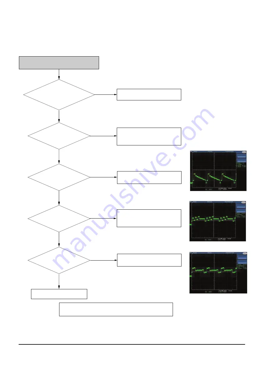
Y(Color-bar)

Pb(Color-bar)

Pr(Color-bar)

# IF Recorder is under PSO(progressive scan output) MODE,
or it does not output the CVBS& S-Video signal.

Component (Y, Cb, Cr) output error

2/4/6 Pin in MCN2

of Jack PCB or CON2 of Main PCB

has normal level?

Analong signals

are inputted normally IC216

(pin 27,28,29)

Power is normal

(5V) at IC216(pin 30,34)

I2C singnal in

IC216(pin16, 18) are swinged

between 0~5V?

Video signal

of About P-P1V appears at

Output Jack?

Check the RCA cable

Check the DIC1 on MAIN PCB

Check the connection between
IC216 and BCN2A(pin5, 6)

Check the connection between
IC216 (pin16,18)
and FIC1 (pin27, 28)

Check the connection between
IC216 and output jack

Check the connection between
pin 2, 4, 6 in MCN2 of Jack
PCB and IC216

No

No

No

No

No

Yes

Yes

Yes

Yes

Yes

Содержание DVD-HR755

Страница 1: ...EU XER NWT AFR AND SMR UMG XSG XFA XSA RAD XSH XSS XST XTL SAM XSE XSV CHN HAC TAW SEO AUS SERVICE Manual ELECTRONICS Samsung Electronics Co Ltd MAY 2007 Printed in Korea AK82 01208A This Service Manual is a property of Samsung Electronics Co Ltd Any unauthorized use of Manual can be punished under applicable international and or domestic law Area Web Site North America URL http service samsungpor...

Страница 2: ...Chassis Product Specification Asia and Austrailia model 2 5 2 5 Option Product Specification 2 7 3 Software Update 3 1 3 4 3 1 Drive Firmware Update 3 1 3 2 Flash Update 3 3 4 Disassembly and Reassembly 4 1 4 8 4 1 Cabinet and PCB 4 1 4 2 PCB Location 4 8 5 Trouble Shooting 5 1 5 14 6 Exploded View and Parts List 6 1 6 4 6 1 Cabinet Assembly 6 2 7 Electrical Parts List 7 1 7 20 7 1 Electrical Part...

Страница 3: ... PCB 11 6 11 5 DV Interface Main PCB 11 7 11 6 MS9400 Codec Main PCB 11 8 11 7 Power Main PCB 11 9 11 8 SAA7138 Video Decoder Main PCB 11 10 11 9 USB Interface Main PCB 11 11 11 10 CEC Jack PCB 11 12 11 11 System Control Jack PCB 11 13 11 12 TM Jack PCB 11 14 11 13 Power Jack PCB 11 15 11 14 Connection Jack PCB 11 16 11 15 I O Jack Jack PCB 11 17 11 16 I O_Switching Jack PCB 11 18 11 17 Display Ke...

Страница 4: ...14 3 About IEEE1394 14 9 If you want to know additional information which is not included on this Service Manual Please refer to the SKP Samsung Knowledge Portal web site URL http service samsungportal com North America URL http latin samsungportal com Latin America URL http cis samsungportal com CIS URL http europe samsungportal com Europe URL http china samsungportal com China URL http asia sams...

Страница 5: ...NSI C101 1 Leakage Current for Appliances and Underwriters Laboratories UL 1270 40 7 With the instrument s AC switch first in the ON position and then in the OFF posi tion measure from a known earth ground metal water pipe conduit etc to all exposed metal parts of the instrument antennas handle brackets metal cabinets screwheads metallic overlays control shafts etc especially any exposed metal par...

Страница 6: ...nched out of place or frayed wiring Do not change spacing between a component and the printed circuit board Check the AC power cord for damage 5 Components parts and or wiring that appear to have overheated or that are otherwise damaged should be replaced with components parts and or wiring that meet original specifications Additionally determine the cause of overheating and or damage and if neces...

Страница 7: ...d lead last 2 The service precautions are indicated or printed on the cabinet chassis or components When servic ing follow the printed or indicated service precau tions and service materials 3 The components used in the unit have a specified flame resistance and dielectric strength When replacing components use components which have the same ratings Components identi fied by shading by or by in th...

Страница 8: ...posure of the assem bly 3 Use only a grounded tip soldering iron to solder or unsolder ESD devices 4 Use only an anti static solder removal devices Some solder removal devices not classified as anti static can generate electrical charges suffi cient to damage ESD devices 5 Do not use freon propelled chemicals These can generate electrical charges sufficient to damage ESD devices 6 Do not remove a ...

Страница 9: ... your hands on the conductive sheet This gives them the same ground as the sheet 4 Remove the optical pick up block 5 Perform work on top of the conductive sheet Be careful not to let your clothes or any other static sources to touch the unit Be sure to put on a wrist strap grounded to the sheet Be sure to lay a conductive sheet made of copper etc Which is grounded to the table Fig 1 3 6 Short the...

Страница 10: ...nalogue AV2 Scart Ext Video Composite RGB Audio analogue Audio Analogue output jacks X 2 Optical coaxial digital audio output Composite Video Video output jack X 1 Output Video S Video output X 1 Y 1 0Vp p C 0 286Vp p at 75 ohm load Component output X 1 Y 1 0Vp p Pb 0 70Vp p Pr 0 70Vp p at 75ohm load HDMI DVI 576P Scart Jack AV1 Scart TV Video Composite RGB Audio analogue Picture compression forma...

Страница 11: ... G B B AV1 Rear Video Composite S Video Audio analogue AV2 Front Video Composite Audio analogue Audio Analogue output jacks X 2 Optical coaxial digital audio output Output Composite Video Video output jack X 1 Video S Video output X 1 Y 1 0Vp p C 0 286Vp p at 75 ohm load Component output X 1 Y 1 0Vp p Pb 0 70Vp p Pr 0 70Vp p at 75ohm load HDMI DVI 576P Picture compression format MPEG II Audio comp...

Страница 12: ...1 L R AV3 Rear Front DV Input Front Yes x1 x1 Aerial Input Rear Yes x 1 x1 x1 RF Out Rear x1 w o Modulator x1 w o Modulator HDMI Output Rear Yes x1 x1 USB2 0 Mass Storage Host Front x1 DVD Video Yes Yes Yes DVD RAM Yes Yes DVD RW O Yes Yes DVD R O Yes Yes DVD RW Yes Yes DVD R Yes Yes VCD Yes w o Logo Yes w o Logo SVCD Yes w o Logo Yes w o Logo MPEG4 DivX3 1 DivX 4 DivX 5 DivX6 Yes Yes DVD Audio SA...

Страница 13: ...P SP LP EP SEP Drive Speed x2 x2 MPEG2 XP SP LP EP 1 2 4 8 1 2 4 8 VIDEO NTSC3 58 REC PB No Q PAL No Q PAL PAL REC PB Yes Yes Yes Yes SECAM REC PB PAL Recording Playback PAL Recording Playback Broadcast System PAL SECAM B G D K I PAL SECAM B G D K I Audio Stereo System A2 NICAM A2 NICAM HDD Capacity 160G 250G 250G 320G RECORDING TIME MODE COLOR SYSTEM TUNER Recording Format ...

Страница 14: ... Front Yes AV3 x 1 AV2 Rear x 1 L R AV1 Front x 1 L R AV2 Rear x 1 Front DV Input Front Yes x 1 Aerial Input Rear Yes x 1 x 1 RF Out Rear x 1 w o Modulator HDMI Output Rear Yes x 1 USB2 0 Mass Storage Host Front x 1 DVD Video Yes Yes DVD RAM Yes DVD RW O Yes DVD R O Yes DVD RW Yes DVD R Yes VCD Yes SVCD Yes MPEG4 DivX3 1 DivX 4 DivX 5 DivX6 Yes DVD Audio SACD CD Yes CD R RW O O Yes MP3 Yes JPEG Ye...

Страница 15: ...cording CD DA MODE XP SP LP EP SEP Drive Speed x2 MPEG2 XP SP LP EP 1 2 4 8 VIDEO NTSC3 58 REC PB No Q PAL PAL REC PB Yes Yes SECAM REC PB PAL Recording Playback Broadcast System PAL SECAM B G D K I Audio Stereo System A2 NICAM HDD Capacity 160G 250G 320G RECORDING TIME MODE COLOR SYSTEM TUNER Recording Format ...

Страница 16: ...teries for Remote Control AK59 00062E 4301 001035 Model Standard of DVD HR755 XEU Model Standard of DVD HR755 XEU S N A Model Standard of DVD HR755 XEU Model Standard of DVD HR755 XEU S N A Model Standard of DVD HR755 XEU Model Standard of DVD HR755 XEU AC39 42001R AC39 00017A Instruction Manual Quick Guide Video Audio Cable RF Cable for TV ...

Страница 17: ...ortal com 2 Write the file to disc using the CD RW of your computer Recommended Application Program Nero Burning Easy CD Creator etc Option Extension name SMD Multisession No Multisession File name lenght Max of 11 8 3 Format Mode 1 Character set ISO 9660 or Joliet Format CD Close Dise at once N O T E Very important please read the notice below before updating your unit The following events may in...

Страница 18: ...n the power again the tray will then close The drive firmware is now complete Atfer checking old and new version select Yes or No with or on the remote control The Version is indicated by XX X modelname You will see LOAD on FLT Display Fig 3 5 1 Press OPEN CLOSE to open the disc tray 2 Insert the update CD R disc with the software update label facing up 3 Press OPEN CLOSE to close the disc tray It...

Страница 19: ...ption Multisession No Multisession CD close disc at once ISO 9660 or joliet format Extension name RUF In order to increase disc playability add a dummy file over 100MB together with the latest program The dummy file can be any kind of file except MP3 file etc which can be played in the unit and we recommend to use a file whose extension name as dmy which can be changed from original one N O T E Ve...

Страница 20: ...ill then close The Flash update is now complete If the message to the left isn t displayed after 10minutes and the unit is no longer functioning properly contact a samsung authorized service center Atfer checking old and new version select Yes or No with or on the remote control The Version is indicated by YYMMDD xx modelname 1 Press OPEN CLOSE to open the disc tray 2 Insert the update CD R disc w...

Страница 21: ...mbly 4 1 Cabinet and PCB 4 1 1 Top Cabinet Removal 1 Remove 5 Screws Œ ˇ 2 Lift up the Top Cabinet in direction of arrow Fig 4 1 Top Cabinet Removal Note Reassembly in reverse order 1 SCREW 3 x 10 B Œ 3 SCREWS 3 x 10 B ˇ 1 SCREW 3 x 10 B TOP CABINET ...

Страница 22: ... Electronics Disassembly and Reaasembly Fig 4 2 Ass y Front Cabinet Removal 4 1 2 Ass y Front Cabinet Removal 1 Release 6 Hooks Œ ˇ and Ass y Front Cabinet ˆ Œ 1 HOOK 2 HOOKS ˇ 2 HOOKS 1 HOOK ˆ ASS Y FRONT CABINET ...

Страница 23: ...eaasembly Samsung Electronics 4 3 4 1 3 Hard Disk Removal 1 Remove 8 Screws Œ ˇ from the Hard Disk and lift it up Fig 4 3 Hard Disk Removal 2 SCREWS NC 8 4 2 Y Œ 4 SCREWS 2 6 x 4 Y ˇ 2 SCREWS 6 32 UNC 8 4 2 Y HARD DISK ...

Страница 24: ...Samsung Electronics Disassembly and Reaasembly 4 1 4 Ass y Deck Removal 1 Remove 4 Screws Œ from the Ass y Deck ˇ and lift it up Fig 4 4 Ass y Deck Removal 2 SCREWS 3 x 10 Y Œ 2 SCREWS 3 x 8 Y ˇ ASS Y DECK ...

Страница 25: ...l 4 1 5 HDMI PCB Main PCB and S M P S PCB Removal 1 Remove 1 Screw Œ from the HDMI PCB and lift it up 2 Remove 2 Screws ˇ from the Main PCB and lift it up 3 Remove 4 Screws ˆ from the S M P S PCB Ø and lift it up Œ 1 SCREW 3 x 10 B HDMII PCB ˇ 2 SCREWS 3 x 10 Y MAIN PCB ˆ 4 SCREWS 3 x 6 Y Ø SMPS PCB ...

Страница 26: ...4 6 Samsung Electronics Disassembly and Reaasembly 4 1 6 Jack PCB Removal 1 Remove 6 Screws Œ from the Jack PCB ˇ and lift it up Fig 4 6 Jack PCB Removal Œ 4 SCREWS 3 x 6 Y ˇ JACK PCB 2 SCREWS 5 x 14 Y ...

Страница 27: ...Disassembly and Reaasembly Samsung Electronics 4 7 4 1 7 DC FAN Removal 1 Remove 2 Screws Œ from the DC Fan and lift it up Fig 4 7 DC FAN Removal DC FAN Œ 2 SCREWS 5 x 14 Y ...

Страница 28: ...4 8 Samsung Electronics Disassembly and Reaasembly 4 2 PCB Location Fig 4 8 PCB Location MAIN PCB S M P S PCB HDMI PCB JACK PCB ...

Страница 29: ... the function key is normal PVDLL1 PSDZ1 PFZZ1 PVZL1 SHOR and OPEN Are normal Is there voitage at Collector of QISO1 Operation of QISO1 is Normal Check feed back ICISO1 Change fuse Change short circuited or opened parts Check 2st voltage Replace QISO1 Change AVFP1 LED Module No No No No No Yes Yes Yes Yes Yes ...

Страница 30: ...tween 0 5V Video signal of About P P1V appears at Output jack Check the RCA cable Check the DIC1 on Main PCB Check the connection between IC216 nad BCN2A pin 5 6 Check the connection between IC216 pin16 18 and FIC1 pin 27 28 IF Recorder is under PSO progressive scan output MODE it does not output the CVBS S Video RGB signal Check the connection between IC216 and output jack Check the connection be...

Страница 31: ... inputted normally IC216 pin 27 28 29 Power is normal 5V at IC216 pin 30 34 I2C singnal in IC216 pin16 18 are swinged between 0 5V Video signal of About P P1V appears at Output Jack Check the RCA cable Check the DIC1 on MAIN PCB Check the connection between IC216 and BCN2A pin5 6 Check the connection between IC216 pin16 18 and FIC1 pin27 28 Check the connection between IC216 and output jack Check ...

Страница 32: ...IC216 pin16 18 are swinged between 0 5V Video signals of about P P1V appears at output jack Check the S Video cable Check the DIC1 on Main PCB Check the connection between IC216 and BCN2A pin5 6 Check the connection between IC216 pin16 18 and FIC1 pin27 28 Check the connection between IC216 and output jack Check the connection between 10pin and 8pin in MCN2 of Jack PCB and IC216 No No No No No Yes...

Страница 33: ...n of SJACK AV1JACK RGB Video signal appears at 7 11 15pin of AV1 output jack Check the RCA cable Check Main PCB Check the connection between IC216 and BCN2A pin5 6 Check the connection between pin 51 of FIC1 and AV1 JACK Check the connection between IC216 and output jack Check the connection between 2 4 and 6pin in MCN2 of Jack PCB and IC216 No No No No No Yes Yes Yes Yes Yes IF Recorder is under ...

Страница 34: ...32 36pin of AV2 RGB control signal level is 4V at 27pin of SJACK AV1JACK Power 5V is nomal at IC216 pin30 34 MCN2 pin 17 19 21 of Jack PCB or CON2 of Main PCB has normal level Check the Scart cable Check the SMPS AL5 8V and BCN2A pin2 3 Check Video out of TV is set RGB mode No No No Yes Yes Yes Yes Check Main PCB ...

Страница 35: ...6 pin16 18 are swinged between 0 5V MCN2 11 of Jack PCB or CON2 of Main PCB has normal level Change Main PCB Check the connection between pin8 in IC216 and AV3 pin jack Check the connection between MCN2 11 of Jack PCB and pin 35 in IC216 Check the connection between IC216 pin16m 18 and FIC1 pin27 28 No No No Yes Yes Yes ...

Страница 36: ...Out Check Current Digital Audio Setting is PCM ChecK Digital Audio data PIN20 of CON2 Main PCB Check 5V SJACK3 Replace SJACK3 Replace Main PCB No No No Yes Yes Check the A V Receiver can Decode Current Bit Steam Set the Bitstream No Yes Yes Check the Cable AUDIO DATA ...

Страница 37: ...ply voltage of VIC1 3 3V Main PCB Check output I2S singnal of audio DAC VDR48 VDR54 VDR55 VDR56 Check the connection between IC216 pin16m 18 and FIC1 pin27 28 Replace Main PCB Replace Main PCB Check the around supply voltage of IC216 No No No Yes Yes Yes Yes Check the passive parts around jack pin Digital clock 10 VDR48 Digital clock 11 VDR54 Digital clock 12 VDR55 Digital clock 15 VDR56 No ...

Страница 38: ...ltage of of VIC13 3V Main PCB Check the audio out signal pin28 29 of CON2 Main PCB Check I2S singnal of audio ADC VDR56 Check the passive parts around Audio Jack pin Replace Main PCB Replace Main PCB Check SMPS No No No Yes Yes Yes Yes Check connection between Main connector CON2 CON3 and Jack connector MCN2 MCN3 No AUDIO DATA VDR56 ...

Страница 39: ...ror Are Main and deck power OK 5v 12v Is the 40pin FFC cable betweenmain deck inserted correctly Is the wavefrom of IC203 pin26 normal Main PCB Check he power Change the Main board Reinsert FFC cable correctly No No No Yes Yes Yes IC203 Pin26 Change the deck ...

Страница 40: ...ed power fortuner is OK pin1 3 5V pin16 33V I2C signal pic11 12 of tuner is OK Video output signal of Tuner is OK jack PCB Tuner line connect TV directly Check between pin 11 12 of tuner and FIC1 Check SMPS AL5 8V and 33V No No No Replace TM tuner block No Yes Yes Yes Yes Refer to AV3 Video line error Tuner Video ...

Страница 41: ...plied power for VIC1 3 3V is OK MAIN PCB 5 5MHz signal from 15 pin of tuner is OK Tuner line connect TV directly Check the SIF signal or tuner Check its power line or around elements No No No Yes Yes Yes If Audio R L signal 30 31pin of NIC1 is normal refer to AV3 Audio Line in error Tuner Audio ...

Страница 42: ...msung Electronics Remocon Not Working FIC1 58pin signal is OK Jack PCB ARM1 pin1 signal is OK Key PCB Check the power pin2 line of ARM1 is 5V Check between FIC1 58pin and ARM1 1pin No No Yes Yes Change AIC1 or around elements ...

Страница 43: ...ng Electronics 6 1 6 Exploded View and Parts List 6 1 Cabinet Assembly DVD HR749 HR750 6 2 Cabinet Assembly DVD HR753 HR754 6 3 Cabinet Assembly DVD HR755 HR756 6 4 Cabinet Assembly DVD HR757 6 2 6 4 6 6 6 8 ...

Страница 44: ...ts List 6 2 Samsung Electronics 6 1 Cabinet Assembly DVD HR749 HR750 P001 W200 W275 W268 W004 W001 W001 W001 W001 W271 W307 W336 W336 C700 C527 C001 A001 P030 P022 P025 P003 H001 C015 P005 C891 VS208 C002 C011 W004 W004 W275 ...

Страница 45: ...P005 AK92 01365A ASSY PCB FUNCTION DVD HR755 HDD 1 SA P022 AK92 01416A ASSY PCB JACK DVD HR750 XEU HDD 1 SA P025 AC39 10019A CBF POWER CORD KKP 419C H03VVH2 F 1 SA P030 3103 001158 FAN DC 12V 20mA 2000rpm 0 125m 3 1 SA VS208 AK39 00086A LEAD CONNECTOR SV R3600 LEAD CONN 1 SA W001 6003 000275 SCREW TAPTITE BH B M3 L10 ZPC 6 SA W004 6003 000283 SCREW TAPTITE BH B M3 L8 ZPC 11 SA W200 6003 001375 SCR...

Страница 46: ...st 6 4 Samsung Electronics 6 2 Cabinet Assembly DVD HR753 HR754 P001 W268 W001 W001 W001 W001 W001 W271 C001 A001 P030 P022 P003 H001 P141 C015 P005 C002 C011 W200 W275 W004 W004 W004 W275 W307 W336 W336 C700 C527 P025 C891 VS208 ...

Страница 47: ...T XER AK92 01364A ASSY PCB SMPS DVD HR755 XEG HDD 1 SA DVD HR754 XEE AK92 01365A ASSY PCB FUNCTION DVD HR755 HDD 1 SA P005 AK92 01365A ASSY PCB FUNCTION DVD HR755 HDD 1 SA AK92 01362A ASSY PCB JACK DVD HR755 XEG HDD 1 SA DVD HR753 XEG EUR XEC XEE XEH XEN XEO XET XEU P022 AK92 01362B ASSY PCB JACK DVD HR755 XEF HDD 1 SA DVD HR753 AUS XEB XEF AK92 01362D ASSY PCB JACK DVD HR755 XEV HDD 1 SA DVD HR75...

Страница 48: ...st 6 6 Samsung Electronics 6 3 Cabinet Assembly DVD HR755 HR756 P001 W268 W001 W001 W001 W001 W001 W271 C001 A001 P030 P022 P003 H001 P141 C015 P005 C002 C011 W200 W275 W004 W004 W004 W275 W307 W336 W336 C700 C527 P025 C891 VS208 ...

Страница 49: ...K92 01364A ASSY PCB SMPS DVD HR755 XEG HDD 1 SA DVD HR756 XEE AK92 01364B ASSY PCB SMPS DVD HR755 XEV HDD 1 SA DVD HR756 XEG P005 AK92 01365A ASSY PCB FUNCTION DVD HR755 HDD 1 SA AK92 01362A ASSY PCB JACK DVD HR755 XEG HDD 1 SA DVD HR755 XEG EUR XEC XEE XEH XEN XEO XET XEU P022 AK92 01362B ASSY PCB JACK DVD HR755 XEF HDD 1 SA DVD HR755 AUS XEB XEF AK92 01362D ASSY PCB JACK DVD HR755 XEV HDD 1 SA D...

Страница 50: ... List 6 8 Samsung Electronics 6 4 Cabinet Assembly DVD HR757 P001 W268 W001 W001 W001 W001 W001 W271 C001 A001 P030 P022 P003 H001 P141 C015 P005 C002 C011 W200 W275 W004 W004 W004 W275 W307 W336 W336 C700 C527 P025 C891 VS208 ...

Страница 51: ...364B ASSY PCB SMPS DVD HR755 XEV HDD 1 SA DVD HR757 XER NWT P005 AK92 01365A ASSY PCB FUNCTION DVD HR755 HDD 1 SA AK92 01370A ASSY PCB JACK DVD HR757 XEG HDD 1 SA DVD HR757 XEC XEE XEG XEH XEN XEO XET P022 XEU AK92 01370B ASSY PCB JACK DVD HR757 XEF HDD 1 SA DVD HR757 AUS XEB XEF AK92 01370D ASSY PCB JACK DVD HR757 XEV HDD 1 SA DVD HR757 XER NWT AC39 10019A CBF POWER CORD KKP 419C H03VVH2 F 1 SA D...

Страница 52: ... 005148 C CER CHIP 100nF 10 16V X7R 1 1 SA MC115 2203 005148 C CER CHIP 100nF 10 16V X7R 1 1 SA MC116 2203 005148 C CER CHIP 100nF 10 16V X7R 1 1 SA MC117 2203 005148 C CER CHIP 100nF 10 16V X7R 1 1 SA MC118 2203 005148 C CER CHIP 100nF 10 16V X7R 1 1 SA MC119 2203 005148 C CER CHIP 100nF 10 16V X7R 1 1 SA MC12 2203 005148 C CER CHIP 100nF 10 16V X7R 1 1 SA MC120 2203 005148 C CER CHIP 100nF 10 16...

Страница 53: ...5148 C CER CHIP 100nF 10 16V X7R 1 1 SA MC9 2203 005148 C CER CHIP 100nF 10 16V X7R 1 1 SA MCK1A 2007 000094 R CHIP 22Kohm 5 1 10W TP 1608 1 SA ME1 2402 001042 C AL SMD 100uF 20 16V GP TP 6 1 SA ME2 2402 001042 C AL SMD 100uF 20 16V GP TP 6 1 SA ME70 2402 001042 C AL SMD 100uF 20 16V GP TP 6 1 SA ME72 2402 001042 C AL SMD 100uF 20 16V GP TP 6 1 SA ME74 2402 001086 C AL SMD 100UF 20 16V WT TP 6 1 S...

Страница 54: ...PR16 2007 000090 R CHIP 10Kohm 5 1 10W TP 1608 1 SA PR17 2007 000070 R CHIP 0ohm 5 1 10W TP 1608 1 SA PR18 2007 001044 R CHIP 56ohm 5 1 10W TP 1608 1 SA PR19 2007 000070 R CHIP 0ohm 5 1 10W TP 1608 1 SA PR2 2007 000073 R CHIP 91ohm 5 1 10W TP 1608 1 SA PR20 2007 001044 R CHIP 56ohm 5 1 10W TP 1608 1 SA PR21 2007 000070 R CHIP 0ohm 5 1 10W TP 1608 1 SA PR22 2007 001044 R CHIP 56ohm 5 1 10W TP 1608 ...

Страница 55: ... VE7 2402 000179 C AL SMD 47uF 20 16V GP TP 6 1 SA VE8 2402 000173 C AL SMD 4 7uF 20 35V GP TP 4 1 SA VE9 2402 000173 C AL SMD 4 7uF 20 35V GP TP 4 1 SA VIC1 1204 002726 IC VIDEO DECODER SAA7138GHL LQ 1 SA VQ01 0501 000341 TR SMALL SIGNAL KSC1623 L NPN 1 SA VR1 3301 001419 BEAD SMD 220ohm 1608 TP 133ohm 1 SA VR12 2007 000659 R CHIP 27OHM 5 1 10W TP 1608 1 SA VR13 2007 000072 R CHIP 47ohm 5 1 10W T...

Страница 56: ... L1S01 AC29 30050B FILTER LINE NOISE 400uH AC 1 SA L1S02 AC29 00002A FILTER LINE NOISE 30mH B 1 SA PCB AK41 00666A PCB SMPS DVD HR755 PHENOL 1 00 1 SNA PCN1 3710 002036 SOCKET BOARD TO BOARD 12P 1R 2 1 SA PCN2 3710 002036 SOCKET BOARD TO BOARD 12P 1R 2 1 SA PCNS6 3711 000240 HEADER BOARD TO CABLE 1WALL 4P 1 SA PPLD1 AH27 00039A COIL CHOKE DR CHOKE 8 6 DVD R 1 SA PPLD2 AH27 00039A COIL CHOKE DR CHO...

Страница 57: ...7R 1 SA AC12 2203 001126 C CER CHIP 0 68nF 10 50V X7R 1 SA AC2 2203 001126 C CER CHIP 0 68nF 10 50V X7R 1 SA AC3 2203 000783 C CER CHIP 0 33nF 5 50V C0G 1 1 SA AC4 2203 000783 C CER CHIP 0 33nF 5 50V C0G 1 1 SA AC5 2203 000491 C CER CHIP 2 2nF 10 50V X7R 1 1 SA ACN5 3708 000181 CONNECTOR FPC FFC PIC 16P 1 25 1 SA AE2 2401 001250 C AL 4 7uF 20 35V GP TP 4x5 5 1 SA AE24 2401 001250 C AL 4 7uF 20 35V...

Страница 58: ...A AR1 2007 000616 R CHIP 24Kohm 5 1 10W TP 1608 1 SA AR11 2007 000616 R CHIP 24Kohm 5 1 10W TP 1608 1 SA AR12 2007 000616 R CHIP 24Kohm 5 1 10W TP 1608 1 SA AR13 2007 001167 R CHIP 75ohm 5 1 10W TP 1608 1 SA AR14 2007 000616 R CHIP 24Kohm 5 1 10W TP 1608 1 SA AR15 2007 000119 R CHIP 560ohm 5 1 10W TP 1608 1 SA ASW1 3404 001261 SWITCH TACT 15V DC 20mA 100gf 1 SA ASW5A 3404 001261 SWITCH TACT 15V DC...

Страница 59: ...hm 5 1 10W TP 1608 1 SA FR9 2001 000273 R CARBON 100KOHM 5 1 8W AA TP 1 SA FX1 2801 003139 CRYSTAL UNIT 8MHz 50ppm 28 AAA 1 SA IC216 1001 001368 IC AV SWITCH HA118827 QFP 56 1 SA IC217 1201 000163 IC OP AMP 4560 SOP 8P 173MIL D 1 SA LD61A AK61 00531A HOLDER LED DVD R145 ABS 94HB T 1 SA MC1 2203 005148 C CER CHIP 100nF 10 16V X7R 1 1 SA MC2 2203 005148 C CER CHIP 100nF 10 16V X7R 1 1 SA MC3 2203 00...

Страница 60: ...AA TP 1 1 SA SR40 2007 001167 R CHIP 75ohm 5 1 10W TP 1608 1 SA SR41 2007 001167 R CHIP 75ohm 5 1 10W TP 1608 1 SA SR42 2007 001167 R CHIP 75ohm 5 1 10W TP 1608 1 SA SR43 2007 000102 R CHIP 100Kohm 5 1 10W TP 160 1 SA SR44 2001 000857 R CARBON 560OHM 5 1 8W AA TP 1 SA SR45 2007 000102 R CHIP 100Kohm 5 1 10W TP 160 1 SA SR46 2001 000857 R CARBON 560OHM 5 1 8W AA TP 1 SA SR47 2001 000857 R CARBON 56...

Страница 61: ... 10 10V X7R 1 1 SA RC15 2203 006048 C CER CHIP 100nF 10 10V X7R 1 1 SA RC16 2203 006048 C CER CHIP 100nF 10 10V X7R 1 1 SA RC17 2203 006048 C CER CHIP 100nF 10 10V X7R 1 1 SA RC21 2203 006048 C CER CHIP 100nF 10 10V X7R 1 1 SA RC22 2404 001020 C TA CHIP 10uF 20 10V GP TP 3 1 SA RC23 2203 006048 C CER CHIP 100nF 10 10V X7R 1 1 SA RC25 2404 001020 C TA CHIP 10uF 20 10V GP TP 3 1 SA RC26 2203 006048 ...

Страница 62: ... 10V X7R 1 1 SA UC24 2203 006048 C CER CHIP 100nF 10 10V X7R 1 1 SA UC25 2203 006048 C CER CHIP 100nF 10 10V X7R 1 1 SA UC26 2203 006048 C CER CHIP 100nF 10 10V X7R 1 1 SA UC27 2203 006048 C CER CHIP 100nF 10 10V X7R 1 1 SA UC28 2404 001020 C TA CHIP 10uF 20 10V GP TP 3 1 SA UC29 2404 001020 C TA CHIP 10uF 20 10V GP TP 3 1 SA UC30 2404 001020 C TA CHIP 10uF 20 10V GP TP 3 1 SA UC31 2203 006048 C C...

Страница 63: ... 000171 R CHIP 0ohm 5 1 16W TP 1005 1 SA UR94 2011 001432 R NET 82ohm 5 1 16W L CHIP 8P 1 SA UR95 2011 001432 R NET 82ohm 5 1 16W L CHIP 8P 1 SA UR96 2011 001432 R NET 82ohm 5 1 16W L CHIP 8P 1 SA UR97 2011 001432 R NET 82ohm 5 1 16W L CHIP 8P 1 SA UR98 2007 000148 R CHIP 10Kohm 5 1 16W TP 1005 1 SA UR99 2007 000070 R CHIP 0ohm 5 1 10W TP 1608 1 SA VC1 2203 006047 C CER CHIP 33nF 10 16V X7R 10 1 S...

Страница 64: ... SNA AK61 00480A BLADE ACT SOH DR3 E5006J L IVO 1 SNA AK97 01860A ASSY FPCB SOH DR4 DVD RECORD 1 SNA 0603 001181 PHOTO DIODE 5 5V 658 79nm 1 SA 0603 001187 PHOTO RECEIVER 6 0V 17 0mA 650 1 SNA 1003 001854 IC DIODE DRIVER EL6939CLZ LPP 1 SA 1404 001328 THERMISTOR NTC 10Kohm 3370K 1 SNA 2007 000070 R CHIP 0ohm 5 1 10W TP 1608 1 SA 2007 000076 R CHIP 330ohm 5 1 10W TP 1608 1 SA 2007 000113 R CHIP 33o...

Страница 65: ...E ETC RF SECAM BOTH MAL 1 SA DVD HR750 XEF AK68 01392E MANUAL USERS DVD HR750 EUR EUR 1 SA DVD HR750 EUR AK68 01392C MANUAL USERS DVD HR750 XEB XEB 1 SA DVD HR750 XEB AK68 01392G MANUAL USERS DVD HR750 XEC XEC 1 SA DVD HR750 XEC AK68 01392J MANUAL USERS DVD HR750 XEE XEE 1 SA DVD HR750 XEE AK68 01392B MANUAL USERS DVD HR750 XEF XEF 1 SA DVD HR750 XEF AK68 01392F MANUAL USERS DVD HR750 XEG XEG 1 SA...

Страница 66: ...This Document can not be used without Samsung s authorization Samsung Electronics 8 1 8 Block Diagrams 8 1 All Block Diagram 8 2 PIC1 TSB4AB1 Block Diagram 8 3 VIC1 SAA7138 Block Diagram 8 2 8 3 8 4 ...

Страница 67: ...Block Diagrams 8 2 Samsung Electronics This Document can not be used without Samsung s authorization 8 1 All Block Diagram Audio Video ...

Страница 68: ...Block Diagrams Samsung Electronics 8 3 This Document can not be used without Samsung s authorization 8 2 PIC1 TSB4AB1 Block Diagram ...

Страница 69: ...Block Diagrams 8 4 Samsung Electronics This Document can not be used without Samsung s authorization 8 3 VIC1 SAA7138 Block Diagram ...

Страница 70: ...Samsung Electronics 9 1 9 Wiring Diagram ...

Страница 71: ...Samsung Electronics 10 1 10 PCB Diagrams 10 1 S M P S PCB 10 2 Main PCB 10 3 Jack PCB 10 4 HDMI PCB 10 5 Function PCB 10 2 10 4 10 6 10 8 10 9 ...

Страница 72: ...PCB Diagrams 10 2 Samsung Electronics 10 1 S M P S PCB COMPONENT SIDE ...

Страница 73: ...PCB Diagrams Samsung Electronics 10 3 CONDUCTOR SIDE ...

Страница 74: ...PCB Diagrams 10 4 Samsung Electronics DIC2 DIC3 DIC1 UIC1 VIC1 10 2 Main PCB COMPONENT SIDE LOC NO X Y VIC1 A 1 UIC1 B 3 DIC1 D 2 DIC3 G 2 DIC2 G 3 ...

Страница 75: ...PCB Diagrams Samsung Electronics 10 5 CONDUCTOR SIDE IC203 RIC2 RIC3 Œ UIC3 UIC4 Œ Flash CS5 LOC NO X Y RIC3 B 0 RIC2 A 1 UIC3 G 2 UIC4 G 3 IC203 F 3 ...

Страница 76: ...PCB Diagrams 10 6 Samsung Electronics FIC4 FIC3 IC216 FIC1 10 3 Jack PCB COMPONENT SIDE LOC NO X Y FIC4 D 1 FIC3 D 1 FIC1 C 1 IC216 C 4 ...

Страница 77: ...PCB Diagrams Samsung Electronics 10 7 IC216 FIC1 FIC3 FIC4 CONDUCTOR SIDE LOC NO X Y FIC4 B 1 FIC3 B 1 FIC1 D 1 IC216 D 5 ...

Страница 78: ...10 4 HDMI PCB CONDUCTOR SIDE IC1 COMPONENT SIDE PCB Diagrams 10 8 Samsung Electronics ...

Страница 79: ...PCB Diagrams Samsung Electronics 10 9 10 5 Function PCB CONDUCTOR SIDE COMPONENT SIDE ...

Страница 80: ...PCB 11 19 HDMI Connector HDMI PCB 11 2 11 3 11 4 11 5 11 6 11 7 11 8 11 9 11 10 11 11 11 12 11 13 11 14 11 15 11 16 11 17 11 18 11 19 11 20 11 21 For schematic Diagram Resistors are in ohms 1 8W unless otherwise noted Note Special note Most semiconductor devices are electrostatically sensitive and therefore require the special handling techniques described under the electrostatically sensitive ES ...

Страница 81: ...ocument can not be used without Samsung s authorization Block Identification of Main PCB IEEE1394 PHY CHIP USB A V DAC ADC MEMORY MPEG ENCODER DECODER I O Block HDMI CEC Block A V Block System Control Servo Block TM Block Power Block Main PCB Jack PCB ...

Страница 82: ...Schematic Diagrams Samsung Electronics 11 3 This Document can not be used without Samsung s authorization 11 1 S M P S SMPS PCB Power ...

Страница 83: ...Schematic Diagrams 11 4 Samsung Electronics This Document can not be used without Samsung s authorization Audio Power Video 11 2 Main Connector Main PCB ...

Страница 84: ...Schematic Diagrams Samsung Electronics 11 5 This Document can not be used without Samsung s authorization Power 11 3 DRAM Main PCB ...

Страница 85: ... Document can not be used without Samsung s authorization Power Œ Œ 11 4 ATAPI Main PCB Œ Flash CS5 These are the waveforms of DVD HR750 DVD HR751 DVD HR753 DVD HR755 DVD HR756 Caution There can be some differences Voltage Frequency stc among cameras ...

Страница 86: ...cument can not be used without Samsung s authorization Power Œ 11 5 DV Interface Main PCB Œ DV IN CLK These are the waveforms of DVD HR750 DVD HR751 DVD HR753 DVD HR755 DVD HR756 Caution There can be some differences Voltage Frequency stc among cameras ...

Страница 87: ...t can not be used without Samsung s authorization Power Audio Video Œ 11 6 MS9400 Codec Main PCB Œ DDR Clock These are the waveforms of DVD 750 DVD HR751 DVD HR753 DVD HR755 DVD HR756 Caution There can be some differences Voltage Frequency stc among cameras ...

Страница 88: ...Schematic Diagrams Samsung Electronics 11 9 This Document can not be used without Samsung s authorization Power 11 7 Power Main PCB ...

Страница 89: ...thorization Power Audio Video Œ ˇ ˆ Ø 11 8 SAA7138 Video Decoder Main PCB Œ CVBS Input PCMO BCK ˇ PCMO LRCLK PCMO Data Out ˆ PCMIO XCLK Ø VIN CLK These are the waveforms of DVD HR750 DVD HR751 DVD HR753 DVD HR755 DVD HR756 Caution There can be some differences Voltage Frequency stc among cameras ...

Страница 90: ...Schematic Diagrams Samsung Electronics 11 11 This Document can not be used without Samsung s authorization Power 11 9 USB Interface Main PCB ...

Страница 91: ...Schematic Diagrams 11 12 Samsung Electronics This Document can not be used without Samsung s authorization Power 11 10 CEC Jack PCB ...

Страница 92: ...Schematic Diagrams Samsung Electronics 11 13 This Document can not be used without Samsung s authorization Power Audio Video 11 11 System Control Jack PCB ...

Страница 93: ...an not be used without Samsung s authorization Power Audio Video Œ 11 12 TM Jack PCB Œ SIF Out of RF Vout of RF These are the waveforms of DVD HR750 DVD HR751 DVD HR753 DVD HR755 DVD HR756 Caution There can be some differences Voltage Frequency stc among cameras ...

Страница 94: ...Schematic Diagrams Samsung Electronics 11 15 This Document can not be used without Samsung s authorization Power 11 13 Power Jack PCB ...

Страница 95: ... not be used without Samsung s authorization Audio Video Power Œ 11 14 Connection Jack PCB Œ IEC958 Digital Audio These are the waveforms of DVD HR750 DVD HR751 DVD HR753 DVD HR755 DVD HR756 Caution There can be some differences Voltage Frequency stc among cameras ...

Страница 96: ...thorization Power Audio Video Ø ˆ Œ ˇ 11 15 I O Jack Jack PCB Œ Y Color bar Pb Color bar ˇ Pr Color bar CVBS Color bar ˆ Y Color bar Ø C Color bar These are the waveforms of DVD HR750 DVD HR751 DVD HR753 DVD HR755 DVD HR756 Caution There can be some differences Voltage Frequency stc among cameras ...

Страница 97: ...Schematic Diagrams 11 18 Samsung Electronics This Document can not be used without Samsung s authorization Power Audio Video 11 16 I O_Switching Jack PCB ...

Страница 98: ...Schematic Diagrams Samsung Electronics 11 19 This Document can not be used without Samsung s authorization Power Audio Video 11 17 Display Key Jack PCB ...

Страница 99: ...Schematic Diagrams 11 20 Samsung Electronics This Document can not be used without Samsung s authorization Power 11 18 Display Key Function PCB ...

Страница 100: ...horization Power Audio Video ˇ ˆ Ø Œ 11 19 HDMI Connector HDMI PCB Œ TMDS Clock I2C Data SPDIF HDMI ˆ VOut Ckock ˇ I2C Clock Ø VOut Data of ITU656 These are the waveforms of DVD HR750 DVD HR751 DVD HR753 DVD HR755 DVD HR756 Caution There can be some differences Voltage Frequency stc among cameras ...

Страница 101: ...Samsung Electronics 12 1 12 Operating Instructions ...

Страница 102: ...Operating Instructions 12 2 Samsung Electronics ...

Страница 103: ...Operating Instructions Samsung Electronics 12 3 ...

Страница 104: ...Operating Instructions 12 4 Samsung Electronics ...

Страница 105: ...Operating Instructions Samsung Electronics 12 5 ...

Страница 106: ...Operating Instructions 12 6 Samsung Electronics ...

Страница 107: ...Operating Instructions Samsung Electronics 12 7 ...

Страница 108: ...Operating Instructions 12 8 Samsung Electronics ...

Страница 109: ...Operating Instructions Samsung Electronics 12 9 ...

Страница 110: ...Operating Instructions 12 10 Samsung Electronics ...

Страница 111: ...h I switch Vin ON OFF Control Vs Ns Vreg REGULATOR Fig 13 1 13 1 2 Circuit description FLY Back RCC Ringing Choke Converter Control a AC Power Rectification Smoothing Terminal 1 BDISO1 Convert AC power to DC Wave rectification 2 CISIO Smooth the voltage converted to DC 3 LISO1 LISO2 LISO4 LISO5 Noise removal at power input output 4 PLRU1 Rush current limit resistance at the momemt of power cord in...

Страница 112: ...voltage to PSDZ1 and PSCX1 and discharges to PSRZ1 PSRZ2 3 PPCF2 For noise removal c PQIZ1 Vcc circuit 1 RIS13 RIS14 RIS15 ICISO1 driving resistance ICISO1 works through driving resistance at power cord in 2 ICISO1 Vcc CISI3 RISI8 DISO3 Use the output of transformer as Vcc because the current starts to flow into transformer while ICISO1 is active Rectify to DISO3 and smooth to CISI3 Use the output...

Страница 113: ...gram Internal Block Diagram of S M P S Circuit Smoothing Circuit Rectified Circuit Line Filter Power IN 220V Noise Removal SNUBBER PWM Control Circuit ICE2BSO1 Converter Voltage Detection Circuit 33V Rectified Smoothing Circuit 5V Rectified Smoothing Circuit 12V Rectified Smoothing Circuit 3 3V Rectified Smoothing Circuit 5V Rectified VoltageCircuit x3 12V Rectified VoltageCircuit O U T P U T X3 F...

Страница 114: ... through error correction code ECC descramble process and error detection code EDC Second WS performs the following processes Delay compensation using Shift register Sample Hold pulse generation I V Gain Control Providing clock for RF chip OPC Control signal generation Lastly PRML completes the adaptive EQ VD and Digital PLL 4 D Chip D Chip consists of Servo DSP DP2 and 1Mbit memory Servo DSP is d...

Страница 115: ... LC98600CT XB0 Built in ATA PI IDE interface supports Ultra DMA modes 0 1 and 2 52x decoding speed 52x encoding speed supported with 33 8688Mhz 1 Maximum transfer speed PIO mode 16 6 MB s with IORDY Ultra DMA 66MB s with DMARQ 2 User can freely set the CD main channel C2 flag and subcode areas in buffer RAM 3 Built in batch transfer function for transferring CD main channel C2 flag etc in a single...

Страница 116: ...utputted via DIC1 MPEG2 Decoder Encoder with video Encoder of digital part 13 3 1 Outline DIC1 MPEG2 Decoder Encoder with video Encoder diverges from the 13 5MHz crystal then generates VSYNC and HSYNC DIC1 MPEG2 Decoder Encoder with video Encoder does RGB encoding copy guard processing and D Aconversion of 10bit Video signal converted into analog signal is outputted via amplifer of analog part DIC...

Страница 117: ... and componect Y Pb Pr to IC216 Y pin31 C pin32 signals are superposed to composited video pin 17 and this signal outputted to Scart AV1 and composite RCA video S video and component video signals are inputted through pin31 s video Y pin33 C pin27 component Y pin28 component Pb pin29 component Pr And IC216 include 6dB amplifier Based on CVBS signal the final output level must be 2Vpp without 75ohm...

Страница 118: ...includes four 10 bit 30 MSPS A D converters and A D conversion of 10bit analog Video signal converted into Digital Video signal ITU R656 Format is outputted via DIC1 MPEG2 Decoder Encoder with video Encoder of digital part The following output formats supply 10 bit 4 2 2 YCbCr to the DIC1 MPEG2 Decoder Encoder with video Encoder of digital part On CVBS and S video inputs the user can control video...

Страница 119: ...AIC9 is syncronized by three Digital clock from DIC1 and output Digital signal to DIC1 Dolby Digital Encoder Decoder 13 4 2 Audio output Block DVD HR755 has four stereo analog line out terminal and two digital output terminal Decoded signal by DIC1 is inputted to AIC1 D A converter then filtered and amplified by IC217 OP amp and finally ouputted via AV switch IC IC216 The Signal outputted via AV2 ...

Страница 120: ...tic of rejection that results in a better band characteristic 5 Mixer IC Mixer OSC PLL It consists a VHF and UHF OSC and Mixer circuit We applied mixer to make better characteristic of rejection it shows especially various beat characteristic 6 PLL IC The PLL IC plays a role selection of Tuner channel It was built in three wire PLL IC charge pump and band driver The minimum of step frequency is 31...

Страница 121: ...ure detection type The carrier which is detected from video det is directly input to AFT The 90 degree delayed phase signal is input at the same time to AFT and the results come out 5 IF AMP IF signal which is selected in Saw filter is amplified in IF amp frequency enough to be detected The IF amp has parallel inputs outputs structure FM Det AFT Lim Amp 1 2 4 5 6 10 11 12 24 21 19 14 15 16 17 Vide...

Страница 122: ...2mm 0 6 2mm Lens NA 0 45 0 45 0 5 0 6 0 6 0 6 Laser wavelenght 780um 780um 650um 650um 650um Track pitch 1 6pm 1 6pm 0 74pm 0 74pm 0 615pm Capacity 0 65GB 0 65GB 4 7GB 4 7GB 4 7GB Track structure Pit train Groove Pit train Groove Land Groove 2 Disc Formats DVD consists of two 0 6mm discs attached together enabling access to the upper and lower side of the disk and 4 sides could be used at maximum ...

Страница 123: ...equires large storage capacity DVD Audio Playback Only High quality sound that exceeds the CD multi channel Audio DVD R 1 Time Recording As with CD R write only once DVD RAM Rewritable This can be virtually used as hard disk with a random more than 100 000 times read write access Rewritable Similar to DVD RAM except than its technology features DVD RW About 1 000 times a separated read write acces...

Страница 124: ...hich enables the user to select the scenario 7 Multi Angle Able to view the camera angle you selected among the scenes recorded with multiple camera angles Note The above media features must have the DVD Title that contains the appropriate contents to function properly 14 2 2 Audio Video Specifications Classification DVD Video Video CD LD Compression MPEG 2 MPEG 1 Analog Pixel 720 x 480 352 x 240 ...

Страница 125: ... Feature 1 When Developing the DVD Software various addition and modification is possible DVD Video uses the variable compresion technology the MPEG 2 to compress the moving image optimally mini mizing the Data loss to Provide a clear natural screen while increasing the storage time DVD Video Feature 2 Application of the MPEG 2 compression technology MPEG 2 Variable compression Max 1 40 Field unit...

Страница 126: ...from leading consumer audio vendors Dolby Digital AC 3 Unlike the traditional Dolby pro Logic method the Dolby Digital method separates all 5 main channels Front L R Center Surround Rear L R and the Sub woofer to provide live surround audio Using the Down Mix method the conventional Dolby Pro Logic and Stereo are all compatible Each separated channels are played back at CD quality sound Frequency ...

Страница 127: ...pansion of viewer selection capabilities 16 9 TV Wide Mode 16 9 Wide Full Screen 4 3 TV Letter Box Mode Pan Scan Mode DVD Video Feature 5 Multi Aspect 4 3 Pan Scan 16 9 Wide 4 3 Letter Box Up to 9 angles of view may be stored enabling the viewer to select a specific viewpoint at a given time Especially for the Music Video and Sports Title this provides a more lively image of the scene DVD Video Fe...

Страница 128: ... Classify the world into 6 regions and if the DVD Title and the Player s Reginal Code do not agree playback is prohibited Regionnal Coding is optional for the Soft developers Region 0 All Code but the Hardware developers must adopt the appropriate regionnal code for sale Region 1 The United States and its territories Canada Region 2 Europe Japan Greenland Egypt South Africa the Middle East Region ...

Страница 129: ... as the conventional LD VCD or Original Film Different Authoring Process are used accoring to the Software developers and this may affect the DVD image quality Authoring Process Remark DVD Video Authoring Process Video Audio Master Surround Audio Master Subtitle Master MPEG 2 Encoding AC 3 MPEG Audio Encoding Cutting Master Disc Production Subtitle Encoding Authoring Process Video Audio Subtitle M...

Страница 130: ... 80 of the bus bandwidth is used for image data and 20 is used for parameter data 3 16 wires are used for data bit transfer and two wires each are used for the separate Line Valid Frame Valid and Pixel Clock signals required with RS 644 transmission A careful comparison of the specifications shown in the table should be your first sele ction guide for the inter face For example for an integ rator ...

Страница 131: ...stom er however technically effective digital cameras may be With the increa sed use of IEEE 1394 in the industrial image processing business many of these problems are solvable in a sure safe and cost effec tive way This example compares two simi lar vision systems Each system uses four Megapixel resolution digital cameras The traditio nal solu tion consists of one frame grabber per camera one pa...

Страница 132: ...uld be mounted using the robots Sin ce thes e camera s had no communication por t for config uration adjusting the AOI was not possible and differ ences in reflection of the parts needed to be adjusted for by driving a flash circuit All cameras were interfaced into one frame grabber one PC Using RS 644 or CameraLink based camera s the customer would need one frame grabber for each camera It is ver...

Отзывы: