
Precautions
1-4
Samsung Electronics
1-3 ESD Precautions
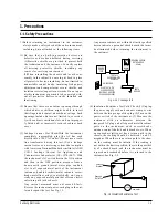
Electrostatically Sensitive Devices (ESD)
Some semiconductor (solid state) devices can be dam-
aged easily by static electricity.
Such components commonly are called Electrostati-
cally Sensitive Devices(ESD). Examples of typical ESD
devices are integrated circuits and some field-effect
transistors and semiconductor chip components. The
following techniques should be used to help reduce
the incidence of component damage caused by static
electricity.
(1) Immediately before handling any semiconductor
component or semiconductor-equipped assembly,
drain off any electrostatic charge on your body by
touching a known earth ground. Alternatively,
obtain and wear a commercially available dis-
charging wrist strap device, which should be
removed for potential shock reasons prior to apply-
ing power to the unit under test.
(2) After removing an electrical assembly equipped
with ESD devices, place the assembly on a conduc-
tive surface such as aluminum foil, to prevent elec-
trostatic charge buildup or exposure of the assem-
bly.
(3) Use only a grounded-tip soldering iron to solder or
unsolder ESD devices.
(4) Use only an anti-static solder removal devices.
Some solder removal devices not classified as
“anti-static” can generate electrical charges suffi-
cient to damage ESD devices.
(5) Do not use freon-propelled chemicals. These can
generate electrical charges sufficient to damage
ESD devices.
(6) Do not remove a replacement ESD device from its
protective package until immediately before your
are ready to install it.(Most replacement ESD
devices are packaged with leads electrically short-
ed together by conductive foam, aluminum foil or
comparable conductive materials).
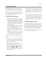
(7) Immediately before removing the protective ma-
terials from the leads of a replacement ESD device,
touch the protective material to the chassis or cir-
cuit assembly into which the device will be
installed.
CAUTION : Be sure no power is applied to the ch-
assis or circuit, and observe all other safety precau-
tions.
(8) Minimize bodily motions when handling unpack-
aged replacement ESD devices. (Otherwise harm-
less motion such as the brushing together of your
clothes fabric or the lifting of your foot from a car-
peted floor can generate static electricity sufficient
to damage an ESD device).
Содержание DVD-C700
Страница 23: ...Reference Information 2 16 Samsung Electronics MEMO ...
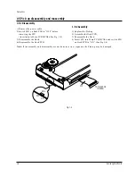
Страница 49: ...4 24 Samsung Electronics Disassembly and Reaasembly MEMO ...
Страница 83: ...Troubleshooting 6 14 Samsung Electronics MEMO ...
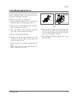
Страница 84: ...Samsung Electronics 7 1 7 Exploded View and Parts List 7 1 Cabinet Assembly 7 2 Deck Assembly Page 7 2 7 4 ...
Страница 89: ...Exploded Views and Parts List 7 6 Samsung Electronics MEMO ...
Страница 101: ...8 12 Samsung Electronics Electrical Parts List MEMO ...
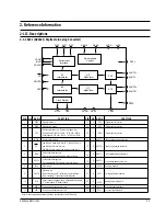
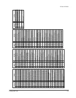
Страница 105: ...PCB Diagrams 10 2 Samsung Electronics 10 1 Main COMPONENT SIDE SOLDER SIDE ...
Страница 106: ...PCB Diagrams Samsung Electronics 10 3 10 2 Jack ...
Страница 107: ...PCB Diagrams 10 4 Samsung Electronics 10 3 S M P S ...
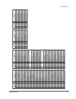
Страница 108: ...PCB Diagrams Samsung Electronics 10 5 10 4 Front COMPONENT SIDE SOLDER SIDE ...
Страница 109: ...PCB Diagrams 10 6 Samsung Electronics 10 5 Key COMPONENT SIDE SOLDER SIDE ...
Страница 110: ...PCB Diagrams Samsung Electronics 10 7 10 6 Head Phone 10 7 Deck COMPONENT SIDE SOLDER SIDE ...
Страница 111: ...PCB Diagrams 10 8 Samsung Electronics 10 8 Sensor 10 9 Motor ...
Страница 113: ...Wiring Diagram 11 2 Samsung Electronics MEMO ...
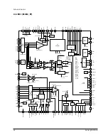
Страница 115: ...Schematic Diagrams 12 2 Samsung Electronics 12 1 S M P S ...
Страница 116: ...Schematic Diagrams Samsung Electronics 12 3 12 2 Main Power Supply ...
Страница 117: ...Schematic Diagrams 12 4 Samsung Electronics 12 3 Main Micom ...
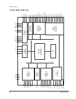
Страница 118: ...Schematic Diagrams Samsung Electronics 12 5 12 4 Servo ...
Страница 119: ...Schematic Diagrams 12 6 Samsung Electronics 12 5 Video Encoder ...
Страница 120: ...Schematic Diagrams Samsung Electronics 12 7 12 6 Video CVBS Output Y Output C Output ...
Страница 121: ...Schematic Diagrams 12 8 Samsung Electronics 12 7 Audio DAC ...
Страница 122: ...Schematic Diagrams Samsung Electronics 12 9 12 8 Audio ...
Страница 123: ...Schematic Diagrams 12 10 Samsung Electronics 12 9 RF ...
Страница 124: ...Schematic Diagrams Samsung Electronics 12 11 12 10 ZiVA ...
Страница 125: ...Schematic Diagrams 12 12 Samsung Electronics 12 11 DSP ...
Страница 126: ...Schematic Diagrams Samsung Electronics 12 13 12 12 Front Micom VFD Display ...
Страница 128: ...Schematic Diagrams Samsung Electronics 12 15 12 14 Head Phone ...
Страница 129: ...Schematic Diagrams 12 16 Samsung Electronics 12 15 Key ...
Страница 130: ...Schematic Diagrams Samsung Electronics 12 17 12 16 Deck ...
Страница 131: ...Schematic Diagrams 12 18 Samsung Electronics 12 17 Deck Control ...
Страница 132: ...Schematic Diagrams Samsung Electronics 12 19 12 18 Remote Control ...
Страница 133: ...Schematic Diagrams 12 20 Samsung Electronics MEMO ...