


TECHNICAL NOTE
Safran Colibrys SA
30N.EVBA V2.10.16
Av. des Sciences 13 – 1400 Yverdon-les-Bains - Switzerland
T +41 58 100 5000
www.safran-colibrys.com
page 4
F +41 58 100 5001
2 Evaluation board function
To facilitate the integration in an user environment and easily verify the excellent performances of the Safran
Colibrys VS1000 serie sensors, the plug and play board EVBA_2.0 integrates one VS1000 sensor with the user
specified range, an ultra-low-noise, high-accuracy 3.3V voltage reference, the decoupling capacitors and output
buffers as shown in Figure 4. The board will powered by a 5V
DC
power supply.
2.1
Normal operation (recommended)
Optimal acceleration measurements are achieved by using the differential buffered signal outputs OUTP_f and
OUTN_f.
2.2
Optional operation
If user application requires a unipolar signal, a single-ended buffered output Vout_SE is provided as well.
2.3
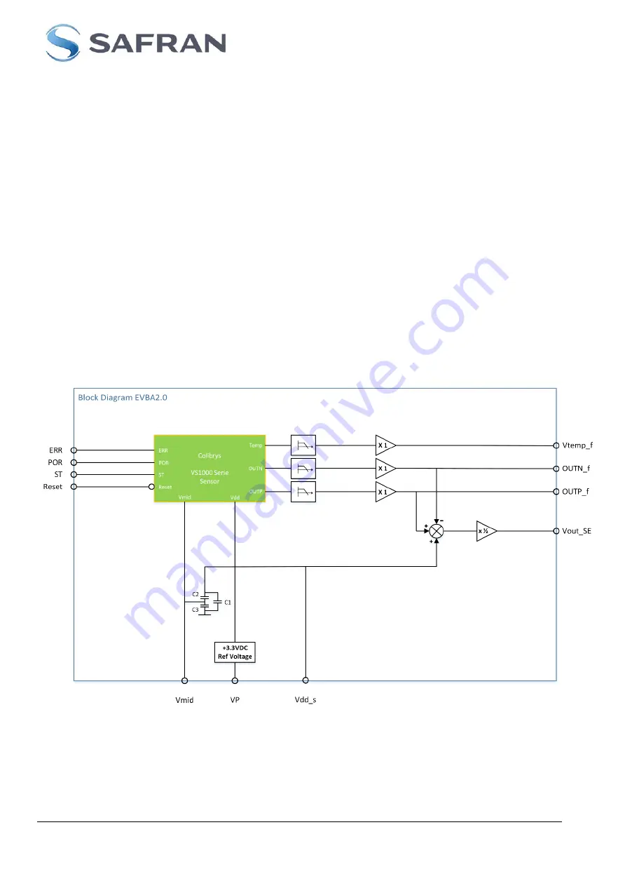
Block Diagram
The Block diagram of the EVBA2.0 is given below. The sensor implemented is represented by the green marked
zone. The VS1000 sensor signal outputs are linked to a unity gain buffer via a 1
st
order low pass filter (fc=16kHz).
The Output of the unity gain buffer is then connected to the dedicated pins of J1. The board +5.0V power supply
is connected to VP and an Ultra-Low-Noise, High-Accuracy 3.3V Voltage Reference generates the necessary
+3.30 VDD voltage. The capacitors C1, C2 and C3 forms the decoupling elements for the ASIC reference voltage
Vmid. Note that this voltage level is also linked to J1. That pin must be left open for normal operation.
The single ended output signal Vout_SE expresses the relation described at §2.8
Figure 4: Functional Diagram EVBA2.0


