Rohde & Schwarz 1152.2518.02 Скачать руководство пользователя страница 69

Interface Description

R&S

®

TS-PCA3

67

User Manual 1152.3908.12 ─ 19
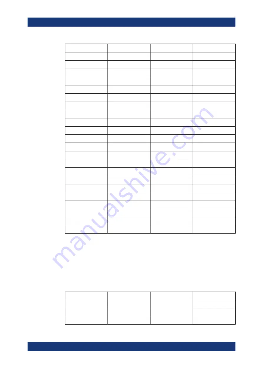
Pin 

1

2

Signal Name

Description

26

M

Reserved

Reserved

27

S

EN#

Enable

28

M

Reserved

3


29

M

NC

Not connected

30

M

V1SENSE

V1 Remote Sense

31

M

Reserved

3


32

N

NC

Not connected

33

M

V2SENSE

V2 Remote Sense

34

M

S RTN

Sense Return

35

M

V1SHARE

V1 Current Share

36

M

V3SENSE

V3 Remote Sense

37

M

Reserved

3


38

M

DEG#

Degrade Signal

39

M

INH#

Inhibit

40

M

Reserved

3


41

M

V2SHARE

V2 Current Share

42

M

FAL#

Fail Signal

43

M

Reserved

3


44

M

V3SHARE

V3 Current Share

45

L

CGND

Chassis Ground

46

M

CAN

AC Input Neutral

47

M

ACL

AC Input Line

1 Pin numbers illustrated are of the female backplane connector

2 L=long length pins, M=medium length pins, S=short length pins

3 For future options

8.1.4


ATX Connectors

Table 8-2: ATX Connector Assignment

Pin

Signal

Signal

Pin

12

V3 Current Share

V2 Current Share

24

11

5 V Sense

3.3 V Sense

23

10

+12 V

+5 V

22

c-PCI-Backplane

Содержание 1152.2518.02

Страница 1: ...R S TS PCA3 Test System Versatile Platform R S CompactTSVP User Manual 1152390812 Version 19 W8...

Страница 2: ...29 0 Email info rohde schwarz com Internet www rohde schwarz com Subject to change data without tolerance limits is not binding R S is a registered trademark of Rohde Schwarz GmbH Co KG Trade names a...

Страница 3: ...Instructions and the product documentation in a safe place and pass them on to the subsequent users Riesgo de lesiones y da os en el instrumento El instrumento se debe usar de manera adecuada para pre...

Страница 4: ...die Produktdokumentation gut auf und geben Sie diese an weitere Benutzer des Produkts weiter Risque de blessures et d endommagement de l appareil L appareil doit tre utilis conform ment aux prescript...

Страница 5: ...mation 15 3 2 Views 17 3 3 Construction 18 3 3 1 Case 18 3 3 2 Slot Layout 20 3 3 2 1 Plan View 20 3 3 2 2 Side View 21 3 3 3 Backplanes 21 3 3 3 1 cPCI Backplane 21 3 3 3 2 Analog Bus Backplane 25 3...

Страница 6: ...5 4 Signal Looping 38 3 4 5 5 Local Signal Outputs 38 3 4 5 6 User CAN Controller 38 3 4 6 Driver Software 39 3 4 7 Self Test 39 3 5 Function Description 39 3 6 Permitted Module Configuration 39 4 Com...

Страница 7: ...nstrument Soft Panels 53 6 Maintenance 54 6 1 Important User Information 54 6 2 Cleaning 54 6 3 Fuse Replacement 55 7 Plug In Modules 56 7 1 General 56 7 2 Configuration Instructions 57 8 Interface De...

Страница 8: ...kplane ATX Connector X12 72 8 3 4 Power Backplane Connector X16 73 8 3 5 Connector X1 P47 73 8 4 Interfaces of the R S TS PSYS1 75 8 4 1 R S TS PSYS1 Connector X1 75 8 4 2 R S TS PSYS1 Connector X20 7...

Страница 9: ...s of the R S TS PCA3 backplane redesign 84 A 1 2 Effects of the TS PCA3 backplane redesign V4 0 84 A 1 2 1 Reason 84 A 1 2 2 Steps taken 85 A 1 2 3 Effects 85 A 1 3 Effects of the versions on individu...

Страница 10: ...Contents R S TS PCA3 8 User Manual 1152 3908 12 19...

Страница 11: ...enable you to use the Test System Ver satile Platform R S TS PCA3 efficiently It consists of the following documents R S TS PCA3 User Manual Software User Manuals R S GTSL R S EGTSL and R S IC Check U...

Страница 12: ...eering practice and the latest scientific and technical findings Nevertheless there are certain risks which cannot be designed out of equipment Additional safety instructions have been developed to pr...

Страница 13: ...User Information R S TS PCA3 11 User Manual 1152 3908 12 19 Highlights important details to which special attention must be paid and that make work easier Explanation of Symbols...

Страница 14: ...ctly connected to a low volt age power supply that also supplies residential buildings Due to occurring grid bound as well as radiated disturbance variables there may be problems to ensure the electro...

Страница 15: ...use fuses supplied by Rohde Schwarz as spare parts or fuses of the same type and rating Shock Hazard The production test platforms R S CompactTSVP and R S PowerTSVP are designed for operating voltages...

Страница 16: ...se they are able to pass signals between each other and select signals under program control and pass them to external measuring systems The peripheral modules can be quickly and flexibly adapted to t...

Страница 17: ...Rear I O is the name given to a design that allows input and output lines of the cPCI connectors P1 and P2 to be accessed from the rear of a backplane Pluggable Rear I O modules can be used for this p...

Страница 18: ...f software packages from the PC sector Table 3 1 Software Standards System Standards Operating system Windows XP Windows 7 Test software LabWindows CVI Visual Studio TestStand Card drivers Drivers bas...

Страница 19: ...with the test devices see Figure 3 4 System serviceability is monitored by a built in self test capability and system monitor operating voltages temperature 3 2 Views Figure 3 2 and Figure 3 3 show t...

Страница 20: ...n R S TS PCA3 18 User Manual 1152 3908 12 19 Figure 3 4 Adapter Interface 3 3 Construction 3 3 1 Case The R S TS PCA3 uses the standard ROHDE SCHWARZ case of the Design 2000 Figure 3 5 BW 2000 Case Co...

Страница 21: ...Side case handles that remain on the unit when mounted in the rack Four rugged detachable rubber feet provide rear protection Unused slots can be covered by front sub panels that maintain the integrit...

Страница 22: ...Description R S TS PCA3 20 User Manual 1152 3908 12 19 3 3 2 Slot Layout 3 3 2 1 Plan View Figure 3 6 Plan View Example Construction...

Страница 23: ...ICMG Power Interface and Rear I O support Analog bus backplane Power backplane with PICMG Power Interface optional Figure 3 8shows the backplanes with the bus systems The assignment of the connec tors...

Страница 24: ...ith Rear I O Voltages up to 125 VDC can be applied at pins provided in the Rear I O area Signals PXI_TRIG0 7 and PXI_CLK10 according to standard PXI R2 0 are available at the P20 connections in slots...

Страница 25: ...the signals of the LBxx It is able to isolate voltages up to 60 V DC PCI slots 3 4 now have this switch in the backplane and are thus CAN capable The CAN bus is continuously connected on slots 15 16...

Страница 26: ...he upper backplane if a screw there connects the backplane signals with the current rail Currently in backplanes V1 1 through V3 0 two pins are hard con nected to carry a higher current This is change...

Страница 27: ...a 26 pin connector X22 and R S switch modules Signals IL1_x and IL2_x Instrument Line are passed from slots 5 to 16 to connector X22 The analog bus signals pass from connector X21 to connector X2 at t...

Страница 28: ...ds on the plug in modules which are used The analog bus concept of the R S TS PCA3 fully meets the requirements that are frequently made in metrology A small number of bus lines for a high number of I...

Страница 29: ...circuit board It can be used to feed as many as 24 signals through the device Ports 5 6 and 7 of the R S TS PIO3B in slot A1 are routed to connector X1 on the rear panel Ports 5 6 and 7 of the R S TS...

Страница 30: ...option offers better screening performance In the second frame CHA GND must not be connected to GND to prevent ground loops The connections are indicated in Figure 3 15 GND sense of 5 V and 3 3 V of t...

Страница 31: ...used in TS PCA3 and TS PWA3 The CAN bus numbering results from the following scheme CANu v w x u Board Number v Controller Number w Device Number x Slot Number Board Number and Controller Number are a...

Страница 32: ...er JP6 open Jumper JP6 closed R S TS PSYS1 R S TS PSYS2 CAN2 User Jumper JP7 open Jumper JP7 closed 3 3 7 Configurations with several Frames or Option R S TS PXB2 In the following figure the terminati...

Страница 33: ...sed in the R S TS PWA3 X10 GA5 can remain set and X11 GA4 can be plugged in the same way as on the main backplane In this way the addressing range of the CAN bus is expanded to slot codes 0000 slot A1...

Страница 34: ...fan unit is especially required if for lack of space slots cannot remain free between modules with DC DC converter module R S TS PDC in the rear IO area or the R S TS PCA3 is not operated in normal ho...

Страница 35: ...vailable in two variants TS PSYS1 1152 4004 02 obsolete TS PSYS1 1157 9910 10 3 4 2 Characteristics Table 3 9 Characteristics of the R S TS PSYS1 R S TS PSYS1 RTM type System functions via CAN node mi...

Страница 36: ...cPCI RTM Rear Transmission Module and is mounted in slot 15 at the rear of the TSVP chassis Connectors X1 and X20 are used to make the connections to the Rear I O side of the cPCI backplane in the R...

Страница 37: ...Description R S TS PCA3 35 User Manual 1152 3908 12 19 Figure 3 19 Connectors and Jumpers on the R S TS PSYS1 1152 4004 02 System Module R S TS PSYS1...

Страница 38: ...S1 see also Figure 3 18 3 4 5 1 Control The R S TS PSYS1 is controlled via CAN The CAN lines are terminated manually with a jumper on the R S TS PSYS1 see Chapter 8 4 Interfaces of the R S TS PSYS1 on...

Страница 39: ...g Inputs A C port reads the status of 4 optocoupler inputs 2 x 2 pin The current at the inputs is limited so that inputs signals can be fed in unconditioned within a wide voltage range These inputs ar...

Страница 40: ...e 75 3 4 5 4 Signal Looping A number of signal lines are looped from connector X30 to connector X20 These are used to input output Rear I O signals e g for the R S switching modules R S TS PMB R S TS...

Страница 41: ...elf Test The module R S TS PSYS1 has no built in self test capability The function of the internal CAN bus can be checked with the local CAN node 3 5 Function Description The functionality of the R S...

Страница 42: ...Description R S TS PCA3 40 User Manual 1152 3908 12 19 Figure 3 21 Module Configuration TS PCA3 Backplane Version 2 1 and 3 x Permitted Module Configuration...

Страница 43: ...User Manual 1152 3908 12 19 Figure 3 22 Module Configuration TS PCA3 The effects of the R S TS PCA3 backplane redesign V4 0 are described in Chap ter A 1 R S TS PCA3 Backplane Versions on page 84 Perm...

Страница 44: ...urces such as presses power punches etc must be avoided The TSVP should be warmed up for approx 15 minutes before measurements commence This time will depend on the type of measuring modules and can b...

Страница 45: ...W 2000 case The R S TS PCA3 can then be pushed into the prepared support in the rack 4 2 3 Desktop Setup When the R S TS PCA3 is set up on a desktop the minimum gap under the unit is provided by the f...

Страница 46: ...without J2 connector all 32 bit standard cPCI modules with without Rear I O and J2 connector in slot 3 and 4 all 32 bit PXI modules in slots 5 to 14 At slot 15 the signal compatibility should be check...

Страница 47: ...hort circuits on the long module so please ensure adequate clearance Tighten the top and bottom screws on the front panel of the plug in module Please observe the following instructions for installati...

Страница 48: ...a 4 4 2 Connections at the Rear Figure 4 1 Rear Connections without Option 1 Knockouts for system and user specific connections 2 Analog bus connections 3 Power connection 4 Slots for Rear I O modules...

Страница 49: ...lattform R S TS PCA3 offers comprehensive opportunities for inner internal and external cabling Inner cabling Cabling by bus systems permanently installed in the R S TS PCA3 PXI Trigger Bus CAN Bus An...

Страница 50: ...bling analog bus to rear connectors 6 PXI Local Bus 7 Cross wiring of short cPCI modules to each other at the front These various cabling options provide a number of benefits Separating the adapter si...

Страница 51: ...Signal injection is generally software controlled 4 5 3 PXI Trigger Bus Plug in modules can be synchronized with the PXI trigger bus The external output of the signals is provided by the system modul...

Страница 52: ...ternal cabling design The cabling to UUT is at the front of the R S TS PCA3 The UUT adapter is located here an adapter interface can also be flange mounted if required The cabling to measuring and sti...

Страница 53: ...ESD electrostatic discharge regulations must be complied with when opening the case of the R S TS PCA3 Figure 4 5 R S TS PCA3 Rear View 1 Case body 2 Rear case feet 4 The case of the R S TS PCA3 must...

Страница 54: ...Commissioning R S TS PCA3 52 User Manual 1152 3908 12 19 The R S TS PCA3 is now accessible from all sides The case is closed in reverse order of opening Cabling...

Страница 55: ...stive protocol generated This is done with the Self Test Support Library The R S TS PSAM module is used as a measurement unit in the TSVP self test The functionality of the modules in the system is en...

Страница 56: ...roducts to clean the R S TS PCA3 Electrical interfaces must not be cleaned with liquid products such as contact spray Depending on the environmental conditions it may be necessary to remove the indivi...

Страница 57: ...built in plug 4 Replace the blown fuses You should identify the cause of the problem and rectify it before replacing the fuse You may be able to tell a blown fuse just by looking at it In case of doub...

Страница 58: ...e 7 1 Plug in modules in the R S TS PCA3 The following types of plug in modules can be used Standard CompactPCI or PXI modules Standard Rear I O modules Extended R S TS PCA3 ATE modules fitted depth 3...

Страница 59: ...e sectional front plate of the short card cannot touch the lines of the adjacent module risk of short circuit The in circuit measuring unit consisting of R S TS PSAM and TS PICT should preferably be c...

Страница 60: ...R S TS PCA3 58 User Manual 1152 3908 12 19 8 Interface Description 8 1 c PCI Backplane 8 1 1 Position of Interfaces Figure 8 1 cPCI Backplane Front View Figure 8 2 Connectors P1 and P20 Front Mating...

Страница 61: ...Figure 8 4 Connectors P1 and P20 Rear Mating Side Note The count sequence is the mirror image of the front 8 1 2 cPCI Connectors 8 1 2 1 General The following tables for the P20 connectors give two si...

Страница 62: ...3 60 User Manual 1152 3908 12 19 8 1 2 2 Slot 1 System BPIO Backpanel I O compatible with 32 bit cPCI CPU s Figure 8 5 Backplane version 4 0 8 1 2 3 Slot 3 and 4 cPCI peripheral NP not populated BP I...

Страница 63: ...Backplane starting with V4 0 SWCAN_H_I and SWCAN_L_I pins C1 and D1 act like BP I O when turned off The CAN bus is turned on with CAN_EN_I via pull up CAN_EN_I is normally on GND or remains open GND...

Страница 64: ...scription R S TS PCA3 62 User Manual 1152 3908 12 19 Figure 8 7 Assignment Slot 5 14 Backplane Version 2 0 to 3 X Change starting with Backplane Version 2 1 12 V and 5 V on front removed isolated c PC...

Страница 65: ...Slot 5 14 Backplane Version 4 X 8 1 2 5 Slot 15 PXI peripheral Rear I O for TS PSYS NC not connected NP not populated BPIO Backpanel I O All signals are output at the back REQ7 GNT7 and CLK7 additiona...

Страница 66: ...escription R S TS PCA3 64 User Manual 1152 3908 12 19 Figure 8 9 Assignment Slot 15 Backplane Version 2 0 to 3 X Change starting with Backplane Version 2 1 12 V and 5 V on front removed isolated c PCI...

Страница 67: ...erface Description R S TS PCA3 65 User Manual 1152 3908 12 19 Figure 8 10 Assignment Slot 15 Backplane Version 4 X 8 1 2 6 Slot 16 CAN NC not connected NP not populated BPIO Backpanel I O c PCI Backpl...

Страница 68: ...0 P47 Figure 8 12 Connector X0 P47 Table 8 1 Assignment X0 P47 Pin 1 2 Signal Name Description 1 4 M V1 V1 Output 5 12 M RTN V1 and V2 Return 13 18 M V2 V2 Output 19 M RTN V3 Return 20 M V3 V3 Output...

Страница 69: ...served3 38 M DEG Degrade Signal 39 M INH Inhibit 40 M Reserved3 41 M V2SHARE V2 Current Share 42 M FAL Fail Signal 43 M Reserved3 44 M V3SHARE V3 Current Share 45 L CGND Chassis Ground 46 M CAN AC Inp...

Страница 70: ...2 3 3 V 12 V 14 1 3 3 V 3 3 V 13 8 1 5 Fan Connectors X90 X91 X92 X93 Table 8 3 Assignment of X90 X93 Pin Signal 4 FANCTRL 3 12 V 2 NC 1 GND 8 1 6 Expansion Connector X80 Table 8 4 Assignment of X80...

Страница 71: ...gnment J1 GA4 J2 PS ON J3 TERM_CAN_H J4 TERM_CAN_L 8 1 8 IPMB0 Table 8 6 IPMBO Assignment Pin Signal 1 IPMB_SCL 2 GND 3 IPMB_SDA 4 IPMB_PWR 5 SMB RSV 8 2 Analog Bus Backplane 8 2 1 Position of Interfa...

Страница 72: ...e 8 7 Assignment of X1 X16 Pin A B C D E 7 IL1_x IL2_x 6 GND 5 ABa1 ABc1 4 ABb1 3 ABb2 ABc2 2 ABa2 1 ABd1 ABd2 Note IL1_x IL1 of the slot 8 2 3 Analog Bus Connector X21 Figure 8 16 Connector X21 Matin...

Страница 73: ...e Table 8 9 Assignment of X22 Pin Signal Pin Signal 1 IL1_5 2 IL2_5 3 IL1_6 4 IL2_6 5 IL1_7 6 IL2_7 7 IL1_8 8 IL2_8 9 IL1_9 10 IL2_9 11 IL1_10 12 IL2_10 13 IL1_11 14 IL2_11 15 IL1_12 16 IL2_12 17 IL1_...

Страница 74: ...ackplane 8 3 2 Power Backplane Utility Connector X13 Table 8 10 Assignment of X13 Pin Signal Signal Pin 1 PRST FAL 6 2 DEG 3 3 V Sense 7 3 3 3 V GND Sense 3 3V 8 4 5V 5V Sense 9 5 GND GND Sense 5V 10...

Страница 75: ...3 3 V 11 8 3 4 Power Backplane Connector X16 Table 8 12 Assignment of X16 Pin Signal 1 V1 Current Share 2 V2 Current Share 3 V3 Current Share 4 NC 8 3 5 Connector X1 P47 Figure 8 19 Connector X1 P47...

Страница 76: ...ected 33 M V2SENSE V2 Remote Sense 34 M S RTN Sense Return 35 M V1SHARE V1 Current Share 36 M V3SENSE V3 Remote Sense 37 M Reserved3 38 M DEG Degrade Signal 39 M INH Inhibit 40 M Reserved3 41 M V2SHAR...

Страница 77: ...TS PCA3 75 User Manual 1152 3908 12 19 8 4 Interfaces of the R S TS PSYS1 8 4 1 R S TS PSYS1 Connector X1 Figure 8 20 R S TS PSYS1 Connector X1 Mating Side Figure 8 21 R S TS PSYS1 Assignment X1 Inter...

Страница 78: ...opulated Figure 8 23 R S TS PSYS1 Assignment X20 8 4 3 R S TS PSYS1 Connector X30 To connect a PowerTSVP to a CompactTSVP only the cable TS PK02 1166 4160 02 is allowed to be used for the TS PSYS2 con...

Страница 79: ...3 5 AUX5 20 4 5 V 35 TRIG4 6 AUX6 21 11 5 V 36 TRIG5 7 TEMP_OUT 22 GND 37 TRIG6 8 OUT1_COM 23 OUT1_NO 38 TRIG7 9 OUT2_COM 24 OUT2_NO 39 CAN2_H 10 OUT3_COM 25 OUT3_NO 40 CAN2_L 11 OUT4_COM 26 OUT4_NO 4...

Страница 80: ...JP6 and JP7 8 4 7 R S TS PSYS1 Jumper JP8 Figure 8 28 Signal at the R S TS PSYS1 Jumper JP8 8 5 External Analog Interface 8 5 1 Analog Bus Connector X2 The analog bus connector X2 is located at the b...

Страница 81: ...d on both sides with the test systems R S CompactTSVP and R S Pow erTSVP Test applications using hazardous active voltages above 30 V r m s and 42 4 V peak or 60 V d c must be operated by a skilled pe...

Страница 82: ...lable at the rear I O slot A4 CAN available if plugged 8 6 2 Rear panel slot A4 CAN Type 9 pin socket Pin Signal 2 CAN_L 3 GND 6 GND 7 CAN_H 9 5V 8 6 3 Rear Panel Slot A4 DIO of Slot A2 Type 25 pin so...

Страница 83: ...IO3 16 A2_P5 IO5 17 A2_P5 IO7 18 A2_P6 IO1 19 A2_P6 IO3 20 A2_P6 IO5 21 A2_P6 IO7 22 A2_P7 IO1 23 A2_P7 IO3 24 A2_P7 IO5 25 A2_P7 IO7 8 6 4 Rear Panel X1 of Slot A1 Type 25 pin socket Pin Signal 1 A1...

Страница 84: ..._P7 IO0 10 A1_P7 IO2 11 A1_P7 IO4 12 A1_P7 IO6 13 GND 14 19 not wired 20 A1_P5 IO1 21 A1_P5 IO3 22 A1_P5 IO5 23 A1_P5 IO7 24 A1_P6 IO1 25 A1_P6 IO3 26 A1_P6 IO5 27 A1_P6 IO7 28 A1_P7 IO1 29 A1_P7 IO3...

Страница 85: ...Data Technical data for the Test System Versatile Platform R S TS PCA3 is specified in the corresponding data sheets If there are discrepancies between the information in this operating manual and the...

Страница 86: ...ing 12 V 5 V front on the rear no more 12 V 5 V on other non critical pins on the rear side CAN bus can only be switched for CAN modules external modules can no longer block CAN bus on other slots AUX...

Страница 87: ...e front of the X20 connector only on the back for details see pin assignment The old R S TS PDC V1 0 serial No 100000 to 100192 must be brought up to the level of V1 1 manually to work with the new ba...

Страница 88: ...here For mechani cal reasons only modules that do not require any rear I O module can be considered Slot 16 Slot 16 is still only suitable for use of R S switching modules with CAN control R S TS PMB...

Страница 89: ...ICT Can also be used in slots 3 and 4 in backplane V4 x caution danger of slot 3 touching the shield springs of the embedded CPU with the module circuit board in slot 3 R S TS PSM1 Can be used in bac...

Страница 90: ...in back plane V4 x also in slots 3 and 4 NOTICE Danger of making contact with front plate slot 2 R S TS PSU Can be used in all versions on slots 5 to 14 in back plane V4 x also in slots 3 and 4 NOTIC...

Страница 91: ...ith V2 1 12 V and part of the 5 V pins are isolated on the front Starting with V4 0 these voltages are completely lacking on the front of the X20 5 V is still available on the rear on other pins non c...

Отзывы: