R01UH0823EJ0100 Rev.1.00
Page 1798 of 1823
Jul 31, 2019
RX23W Group
51. Electrical Characteristics
Note:
The characteristics apply when no pin functions other than A/D converter input are used. Absolute accuracy includes
quantization errors. Offset error, full-scale error, DNL differential non-linearity error, and INL integral non-linearity error do not
include quantization errors.
Note 1. The conversion time is the sum of the sampling time and the comparison time. As the test conditions, the number of sampling
states is indicated.
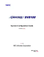
Figure 51.58
Equivalent Circuit
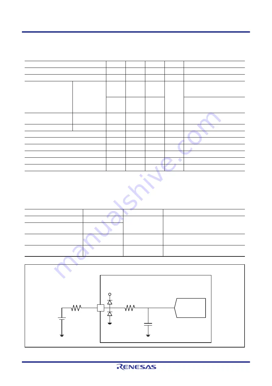
Table 51.44
A/D Conversion Characteristics (5)
Conditions: 1.8 V ≤ VCC = VCC_USB = AVCC0 = VCC_RF = AVCC_RF ≤ 3.6 V, 1.8 V ≤ VREFH0 ≤ AVCC0,
VSS = AVSS0 = VSS_USB = 0 V, reference voltage = VREFH0 selected, T
a
= –40 to +85°C
Item
Min.
Typ.
Max.
Unit
Test Conditions
Frequency
1
—
8
MHz
Resolution
—
—
12
Bit
Conversion time*
(Operation at
PCLKD = 8 MHz)
Permissible signal
source impedance
(Max.) = 5 kΩ
6.75
—
—
μs
High-precision channel
The ADCSR.ADHSC bit is 1
The ADSSTRn register is 0Dh
10.13
—
—
Normal-precision channel
The ADCSR.ADHSC bit is 1
The ADSSTRn register is 28h
Analog input capacitance
Cs
—
—
15
pF
Pin capacitance included
Figure 51.58
Analog input resistance
Rs
—
—
2.5
kΩ
Offset error
—
±1
±7.5
LSB
Full-scale error
—
±1.5
±7.5
LSB
Quantization error
—
±0.5
—
LSB
Absolute accuracy
—
±3.0
±8.0
LSB
DNL differential non-linearity error
—
±1.0
—
LSB
INL integral non-linearity error
—
±1.25
±3.0
LSB
Table 51.45
A/D Converter Channel Classification
Classification
Channel
Conditions
Remarks
High-precision channel
AN000 to AN007
AVCC0 = 1.8 to 3.6 V
Pins AN000 to AN007 cannot be used as digital
outputs when the A/D converter is in use.
Normal-precision channel
AN016 to AN020,
AN027
Internal reference voltage input
channel
Internal reference
voltage
AVCC0 = 2.0 to 3.6 V
Temperature sensor input channel Temperature sensor
output
AVCC0 = 2.0 to 3.6 V
12b - ADC
Cs
Rs
R0
MCU


