background image

Emulation Adapter 

Names and Functions of Hardware 

R20UT4460EJ0110  Rev. 1.10 


Page  22  of  53 

Nov. 01, 2019 


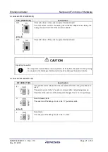
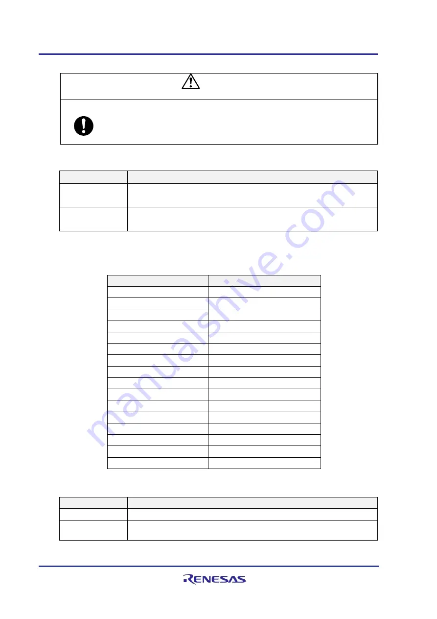
CAUTION


Operating the switch: 


Do not operate a switch before removing static electricity from the operator’s body. Doing 
so may lead to the discharge of static electricity and so damage the internal circuits. 


(4)


Status LEDs: LED1 (3.3 V) and LED2 (5 V) 

Name of LED 

Specification 

LED1 (3.3 V) 

Illuminated: The 3.3-V power supply on the base board is on. 

Not illuminated: The 3.3-V power supply on the base board is off. 

LED2 (5 V) 

Illuminated: The 5-V power supply on the base board is on. 

Not illuminated: The 5-V power supply on the base board is off. 


(5)


Jumper blocks: JP1 to JP16 (selecting each of the power-supply voltages) 

The target power-supply voltages for each of these jumper blocks are listed below. 

JP 

Target Power-Supply Voltage 

JP1 

ADSVCC 

JP2 

ADSVRFFH 

JP3 

A0VCC 

JP4 

A1VCC 

JP5 

A2VCC 

JP6 

A3VCC 

JP7 

A0VREFFH 

JP8 

A1VREFFH 

JP9 

A2VREFFH 

JP10 

A3VREFFH 

JP11 

E0VCC 

JP12 

E1VCC 

JP13 

E2VCC 

JP14 

LVDVCC 

JP15 

SYSVCC 

JP16 

VCC 


Each jumper block has common specifications as shown in the following table. 

JP1 to JP11 

Specification 

Open-circuit 

The target power-supply voltage is off. 

1-2 short-circuit 
(default) 

5 V is supplied as the target power-supply voltage. 


Содержание RTE7702012EAB00000J

Страница 1: ...rials including products and product specifications represents information on the product at the time of publication and is subject to change by Renesas Electronics Corp without notice Please review the latest information published by Renesas Electronics Corp through various means including the Renesas Electronics Corp website http www renesas com www renesas com ...

Страница 2: ...onics with respect to maximum ratings operating power supply voltage range heat dissipation characteristics installation etc Renesas Electronics disclaims any and all liability for any malfunctions failure or accident arising out of the use of Renesas Electronics products outside of such specified ranges 7 Although Renesas Electronics endeavors to improve the quality and reliability of Renesas Ele...

Страница 3: ... products please see the user s manuals additional documents for user s manuals and application notes provided for the individual products When you use an emulator from another company for debugging be sure to read the user s manual for the given emulator Related Documents Name of Document Document No IE850A Emulator RTE0T0850AKCT00000J User s Manual R20UT4461E E2 Emulator RTE0T00020KCE00000R User...

Страница 4: ...provide workarounds for and correct trouble with products malfunctions with some free and some incurring charges However this does not necessarily mean that Renesas Electronics Corp guarantees the provision of a workaround or correction under any circumstances 4 The product covered by this document has been developed on the assumption that it will be used for program development and evaluation in ...

Страница 5: ...e of this product Therefore the specification or design of this product or this user s manual may be changed without prior notice About rights 1 We assume no responsibility for any damage or infringement on patent rights or any other rights arising from the use of any information products or circuits presented in this user s manual 2 The information or data in this user s manual does not implicitl...

Страница 6: ...ere WARNING WARNING indicates a potentially dangerous situation that will cause death or heavy wound unless it is avoided CAUTION CAUTION indicates a potentially dangerous situation that will cause a slight injury or a medium degree injury unless it is avoided To avoid a possible danger the following diagrammatic symbols are used to call your attention means WARNING or CAUTION Example CAUTION AGAI...

Страница 7: ...gged may be destroyed Make sure that the connectors and cables are connected in the correct directions Neglect of this precaution will result in getting an electric shock or will result in this product emitting smoke or catching fire Warning for Modification Do not modify this product Personal injury due to electric shock may occur if the product is modified Modifying the product will void your wa...

Страница 8: ...tor and the target system 2 After a lapse of 10 seconds turn on the power of this product again then launch the emulator debugger Caution to Be Taken for Disposal Penalties may be applicable for incorrect disposal of this waste in accordance with your national legislation European Union Regulatory Notices The WEEE Waste Electrical and Electronic Equipment regulations put responsibilities on produc...

Страница 9: ...version Adapter RTE0T00020KCA30000J 25 2 4 Power Supply Cable 26 2 5 Demounting Lever 27 3 System Configuration and Setup 28 3 1 System Configuration as a Simple Evaluation Board 28 3 2 System Configuration as an Emulation Board 33 4 Notes 39 4 1 Setting Option Bytes 39 4 2 Notes on Differences between the Actual Device and the Emulation Adapter 39 5 Characteristics of Target Interface 41 6 Mainte...

Страница 10: ...d communications protocol from Xilinx Inc The debug chip is capable of using Aurora as a trace interface Target system This means the user created system which is to be debugged This includes both hardware and software created by the user Emulation adapter This is a board which emulates the device to be debugged A debug chip is mounted on the board Base board This board is for operating the emulat...

Страница 11: ...lator which supports Aurora tracing such as the IE850A emulator type name RTE0T0850AKCT00000J from Renesas enables debugging Using the attached 34 pin to 14 pin conversion connector enables connecting the emulation adapter to on chip debugging emulators and flash programmers such as the E2 emulator type name RTE0T00020KCE00000R from Renesas The emulation adapter can operate as a stand alone unit i...

Страница 12: ...e emulated 468 pin BGA RH850 E2UH 468 pin BGA RH850 E2H 373 pin BGA RH850 E2H Power supply for the emulation adapter 4 5 V min 5 0 V typ 5 5 V max External dimension Emulation adapter 47 mm x 51 mm Base board 100 mm x 120 mm Weight Emulation adapter 22 g Base board 79 g Operating temperature 0 to 40 C no condensation Storage temperature 15 to 60 C no condensation EMC EU EN55032 Class A EN55024 USA...

Страница 13: ...esponsible for placing on the market Name Renesas Electronics Europe GmbH Address Arcadiastrasse 10 40472 Dusseldorf Germany Trademark and Type name Trademark Renesas Product name RH850 E2x FCC2 Emulation adapter Base board Type name RTE7702012EAB00000J Environmental Compliance and Certifications Waste Electrical and Electronic Equipment WEEE Directive 2012 19 EU United States Regulatory notices o...

Страница 14: ...dance with the instruction manual may cause harmful interference to radio communications Operation of this equipment in a residential area is likely to cause harmful interference in which case the user will be required to correct the interference at his own expense This device complies with Part 15 of the FCC Rules Operation is subject to the following two conditions 1 this device may not cause ha...

Страница 15: ... of usage 2 1 Emulation Adapter RTE7702012EAB00000J An emulation adapter is an emulation board on which the debug chip is mounted Using the emulation adapter with the exchange adapter allows connection to the target system The emulation adapter can also be used as a simple evaluation board in combination with the attached base board Figure 2 1 Names of the Parts of the Emulation Adapter RTE7702012...

Страница 16: ... 11 12 TRST TODP2 13 14 MD0 TODN2 15 16 EVTI GND 17 18 EVTO TODP3 19 20 MD1 TODN3 21 22 RESET GND 23 24 GND MSYNZ 25 26 CICREFP WDTDIS 27 28 CICREFN GND 29 30 GND BREQ 31 32 DRDY BGNT 33 34 RESOUT 3 Power supply connector CN2 CN2 is connected to the power supply cable that comes with this product or that comes with the IE850A When a base board is connected and emulation RAM ERAM or external tracin...

Страница 17: ...stics into consideration an oscillator on the target system is not used the oscillator in this socket is used instead Change the oscillator in the socket if this is required 5 Jumper blocks JP2 CLGMD1 and JP1 CLGMD0 JP2 CLGMD1 JP1 CLGMD0 Specification Open circuit default Open circuit default 400 MHz mode Open circuit Short circuit Settings prohibited Short circuit Open circuit Short circuit Short...

Страница 18: ...must be made when the emulation adapter is to be connected to the base board 2 3 short circuit VDD on the target system is supplied as VDD for the debug chip When this setting is to be used refer to notes in section 4 2 3 JP4 EMUVCC JP5 EMUVDD Specification Open circuit Open circuit Setting prohibited EMUVCC OFF EMUVDD always ON Open circuit 1 2 short circuit Setting prohibited EMUVCC OFF EMUVDD O...

Страница 19: ... EMUVDD Illuminated EMUVDD ON Not illuminated EMUVDD OFF 11 Interfaces for the exchange adapter CN10 CN11 CN12 and CN13 These connectors are used to connect an exchange adapter or the base board CN10 has a different shape from the others to prevent erroneous insertion 12 Pin header JP8 JP8 is a pin header for the AUD R pin 13 Sticker for aligning the position of pin 1 This mark indicates the posit...

Страница 20: ...Figure 2 2 Names of the Parts of the Base Board RTE7702012EABBB000J 1 Interfaces for the exchange adapter CN10 CN11 CN12 and CN13 These connectors are used for connection to the emulation adapter CN10 has a different shape from the others to prevent erroneous insertion These connectors are connected to CN10 CN11 CN12 and CN13 of the emulation adapter Top view 1 Interfaces for the exchange adapter ...

Страница 21: ... switch Do not operate a switch before removing static electricity from the operator s body Doing so may lead to the discharge of static electricity and so damage the internal circuits 3 Switch SW2 RESET SW SW2 RESET SW Specification L This position starts release from the reset state after the debug chip has been reset The switch returns to the H position a moment after it stops being pressed The...

Страница 22: ...lluminated The 5 V power supply on the base board is on Not illuminated The 5 V power supply on the base board is off 5 Jumper blocks JP1 to JP16 selecting each of the power supply voltages The target power supply voltages for each of these jumper blocks are listed below JP Target Power Supply Voltage JP1 ADSVCC JP2 ADSVRFFH JP3 A0VCC JP4 A1VCC JP5 A2VCC JP6 A3VCC JP7 A0VREFFH JP8 A1VREFFH JP9 A2V...

Страница 23: ...plied as the target power supply voltage 6 Jumper block JP17 MD0 JP17 MD0 Specification Open circuit default MD0 pin L pulled down Short circuit MD0 pin H pulled up 7 Jumper block JP18 MD1 JP18 MD1 Specification Open circuit default MD1 pin L pulled down Short circuit MD1 pin H pulled up 8 Silk screened mark for aligning the position of pin 1 When connecting the emulation adapter match the positio...

Страница 24: ...P00_7 P00_8 P00_9 P21_2 P22_13 P22_12 10 20 AN373 P00_10 P00_11 P22_9 P22_10 P22_11 11 19 AN372 AN371 AN370 P22_8 P22_7 P22_6 12 18 AN303 AN302 AN301 P22_3 P22_4 P22_5 13 17 AN313 AN312 AN300 P22_2 P22_1 P22_0 14 16 AN323 AN311 AN310 NC NC NMI 15 15 AN322 AN321 AN320 NC GND GND 16 14 AN363 AN362 AN361 P23_5 P23_6 P23_7 17 13 AN353 AN352 AN360 P23_4 P23_3 P23_2 18 12 AN273 AN351 AN350 P25_0 P23_0 P...

Страница 25: ...ation adapter 2 Connector CN2 14 pin side CN2 is a 14 pin connector that is defined as a connector for the RH850 emulators This connector can be connected to on chip debugging emulators such as the E2 emulator type name RTE0T00020KCE00000R from Renesas and flash programmers that support the 14 pin connector The following shows pin assignments of CN2 Read the user s manual for the emulator you will...

Страница 26: ...e emulation adapter 2 Power jack J1 red Supply 5 V from a stabilized power supply 3 Power jack J2 black Connect J2 to GND 4 Tabs for unlocking the connector When disconnecting the power supply cable from the emulation adapter press the tabs on both sides of the CN1 connector of the power supply cable to unlock the connector CAUTION Unlocking the connector Do not press the tabs for unlocking the co...

Страница 27: ...Lever To remove the emulation adapter from the base board or exchange adapter insert the demounting lever alternately below all four corners of the emulation adapter and gradually pull the emulation adapter out CAUTION Point for caution on removing the emulation adapter When you remove the emulation adapter from the base board or exchange adapter take care not to damage or deform peripheral compon...

Страница 28: ...tion board See section 3 1 An emulation board See section 3 2 3 1 System Configuration as a Simple Evaluation Board Figure 3 1 shows a system configuration when the emulation adapter is connected to the base board for use as a simple evaluation board Connection of an emulator is not essential Using the pin headers on the base board enables the control and monitoring of each pin of the target devic...

Страница 29: ...aking JP2 and JP1 open circuit Refer to 5 in section 2 1 Jumper block JP3 ICE We recommend making JP3 open circuit Refer to 6 in section 2 1 Jumper blocks JP4 EMUVCC and JP5 EMUVDD We recommend making JP4 and 1 2 on JP5 short circuit Refer to 7 in section 2 1 Jumper block JP6 AURORES We recommend making 1 2 on JP6 short circuit Refer to 8 in section 2 1 Jumper block JP7 VDD Be sure to make 1 2 on ...

Страница 30: ...supplied by connecting the power supply cable attached to the IE850A 3 Connecting the emulation adapter to the base board Connect the two boards so that the sticker and silk screened mark for aligning the positions of pin 1 of the emulation adapter and base board are in the same position 4 Connecting the emulator only if you are using an emulator Connect the emulator to the CN1 connector for exter...

Страница 31: ...ogram When the emulator is connected the debug chip will be kept in the reset state before execution of a program is started by the debugger after the debugger has been launched although this depends on the specifications of the emulator CAUTION Applied voltage Make sure that the voltage applied to CN2 is within the specified range 4 5 V to 5 5 V An applied voltage out of the range may cause the e...

Страница 32: ...d 4 Disconnecting the emulator only if you are using an emulator Disconnect the emulator from the emulation adapter 5 Disconnecting the emulation adapter from the base board To disconnect the emulation adapter from the base board insert the demounting lever which comes with this product into alternate corners among the four corners between the two boards and gradually pull the emulation adapter ou...

Страница 33: ...lation Board Figure 3 2 shows a system configuration when the emulation adapter is to be connected to the exchange adapter then connected to a target board the base board is not used For the specifications of the exchange adapter refer to appendix A Specifications of the Exchange Adapter Figure 3 2 System Configuration Emulation Board ...

Страница 34: ...ion This connector is for mounting on the target system Exchange adapter required for emulation This conversion adapter is for connecting the emulation adapter to the target connector CSSOCKET space adapter optional This adapter is used to adjust the height It is an optional product which is available for use if the components around the target connector would otherwise touch the exchange adapter ...

Страница 35: ...dapter When an emulator is not in use Leave the connector open circuit Power supply connector CN2 Set up a 5 V supply through the attached power supply cable If you are using the IE850A power can be supplied from the power supply cable attached to the IE850A Clock socket X1 An oscillator is mounted 40 MHz at shipment When you are evaluating the emulation adapter with a main oscillator that has a d...

Страница 36: ... block JP7 VDD Be sure to make 2 3 on JP7 short circuit Refer to 9 in section 2 1 Interfaces for the exchange adapter CN10 CN11 CN12 and CN13 Connect these connectors to the exchange adapter 3 2 3 Procedure for Setting the Emulation Adapter up as an Emulation Board This section describes the procedure for setting the emulation adapter up for use as an emulation board 1 Settings on the boards Make ...

Страница 37: ...apter CAUTION Connecting the emulator Confirm the direction with the notch on the connector and connect the emulator while taking care that the direction of insertion is correct 6 Turning on the emulator only if you are using an emulator Turn on the emulator For details refer to the manuals for the emulator you are using 7 Turning on the emulation adapter Output 5 V from the power supply unit that...

Страница 38: ...he exchange adapter To disconnect the emulation adapter from the exchange adapter insert the demounting lever which comes with this product into alternate corners among the four corners between the two boards and gradually pull the emulation adapter out Take care of the positions where you insert the demounting lever so that you do not accidentally tear off components on the boards For details ref...

Страница 39: ... FFF8H for emulation of the E2H 4 1 2 OPBT3 OPBT3 defines the CPUs which are to be enabled Since the debug chip emulates the E2UH which has six CPUs disable the unnecessary CPUs set the PEx_DISABLE to 1 through the setting of OPBT3 4 2 Notes on Differences between the Actual Device and the Emulation Adapter 4 2 1 Current Drawn When the emulation adapter is in use current drawn may differ from that...

Страница 40: ...you use the power supply from the target system note that transient drops in the power supply voltage may occur 4 2 4 VSS Pins for Each Power Supply Voltage AxVSS ADSVSS and VSS are connected to a common GND in the emulation adapter 4 2 5 RAMSVCL and ADSVCL Pins Stabilizing capacitors are connected to the stabilizing capacitor connection pins RAMSVCL and ADSVCL on the emulation adapter These pins ...

Страница 41: ...ExVCC LVDVCC NMI ERROROUT_M VDD VCC GND TCK TMS TDI TDO TRST EVTO EVTI DRDY MD0 1 RES_IN RES_OUT Pow er generation circuit VDD EMUVDD EMUVCC VDD_POK EMUVDD_POK Debug chip IC1 Pow er control circuit VDD_EN EMUVDD_EN JP4 JP5 Pxx_xx ANxxx AxVCC ADSVCC AxVREFH ADSVREFH ADSVREFHL SYSVCC ExVCC LVDVCC NMI ERROROUT_M VDD EMUVDD EMUVCC VCC XTAL EXTAL RAMSVCL ADSVCL AUDCK AUDSYNC AUDRST AUDATA0 3 CLGMD0 CLG...

Страница 42: ...of the product after purchase such as dropping the product while it is being transported or otherwise moved c Failure or damage to the product caused by other pieces of equipment connected to it d Failure or damage attributable to fire earthquakes thunderbolts floods or other natural disasters or to abnormal voltages etc e Failure or damage attributable to modifications repairs adjustments or othe...

Страница 43: ... product to us for repair are at your own expense 6 4 How to Request Repairs If your product is found faulty fill in a Repair Request Sheet downloadable from the following URL and email the sheet and send the product to your local distributor http www renesas com repair CAUTION Note on Transporting the Product When sending your product for repair use the packing box and cushioning material supplie...

Страница 44: ...oration Table A 1 Exchange Adapters and Sockets for the Packages of the Target Devices 3 Number of insertions and removals of the connector The connector is guaranteed for correct insertion and removal 100 times 4 How to use the emulation adapter The emulation adapter can be connected to the target system via the exchange adapter through the following procedure Align the positions of pin 1 as show...

Страница 45: ...Emulation Adapter Appendix A Specifications of the Exchange Adapter R20UT4460EJ0110 Rev 1 10 Page 45 of 53 Nov 01 2019 Figure A 1 Connecting the Emulation Adapter ...

Страница 46: ...x A Specifications of the Exchange Adapter R20UT4460EJ0110 Rev 1 10 Page 46 of 53 Nov 01 2019 5 Dimensions Figure A 2 Dimensions of the RTE7702012CBG468T000J 468 pins Figure A 3 Dimensions of the RTE7702011CBG373T000J 373 pins ...

Страница 47: ...change Adapter R20UT4460EJ0110 Rev 1 10 Page 47 of 53 Nov 01 2019 6 Drawing of the assembly Figure A 4 Drawing of the Assembly for the RTE7702012CBG468T000J 468 pins Figure A 5 Drawing of the Assembly for the RTE7702011CBG373T000J 373 pins Unit mm Unit mm ...

Страница 48: ...Emulation Adapter Appendix A Specifications of the Exchange Adapter R20UT4460EJ0110 Rev 1 10 Page 48 of 53 Nov 01 2019 7 Characteristics of the target interface Figure A 6 Equivalent Circuit ...

Страница 49: ...end an email to the address below Tokyo Eletech Corporation http www tetc co jp e_index htm Disposal Instruction This is only valid in the European Union The WEEE Waste Electrical and Electronic Equipment regulations put responsibilities on producers for the collection and recycling or disposal of electrical and electronic waste Return of WEEE under these regulations is applicable in the European ...

Страница 50: ...mulation Adapter for the RH850 E2UH and E2H Groups User s Manual Rev Date Description Page Summary 1 00 Dec 01 2018 First Edition issued 1 10 Nov 01 2019 11 15 The type name of debug chip was changed from R7F702Z10ADBG to R7F702Z10AADBG ...

Страница 51: ...Colophon Emulation Adapter for the RH850 E2UH and E2H Groups User s Manual Publication Date Rev 1 00 Dec 01 2018 Rev 1 10 Nov 01 2019 Published by Renesas Electronics Corporation ...

Страница 52: ...onics Shanghai Co Ltd Unit 301 Tower A Central Towers 555 Langao Road Putuo District Shanghai 200333 P R China Tel 86 21 2226 0888 Fax 86 21 2226 0999 Renesas Electronics Hong Kong Limited Unit 1601 1611 16 F Tower 2 Grand Century Place 193 Prince Edward Road West Mongkok Kowloon Hong Kong Tel 852 2265 6688 Fax 852 2886 9022 Renesas Electronics Taiwan Co Ltd 13F No 363 Fu Shing North Road Taipei 1...

Страница 53: ...R20UT4460EJ0110 Back Cover Emulation Adapter for the RH850 E2UH and E2H Groups RTE7702012EAB00000J User s Manual ...

Отзывы: