R20UT3282ED0101 Rev. 1.1
7
2015-06-10
3.2
Voltage distribution
The table shows the required device power supply pins. For detailed explanation
of their function, please refer to the user documentation of the corresponding
device:
Device Supply Pin
SYSVCC
VCC
EnVCC (n = 0, 1)
AnVCC (n = 0, 1)
AnVREFH (n = 0, 1)
VDD (VCL)
Additional one power supply for the MainBoard can be selected:
Supply voltage
Function
VDDIOF
IO supply voltage for components located on a
connected mainboard.
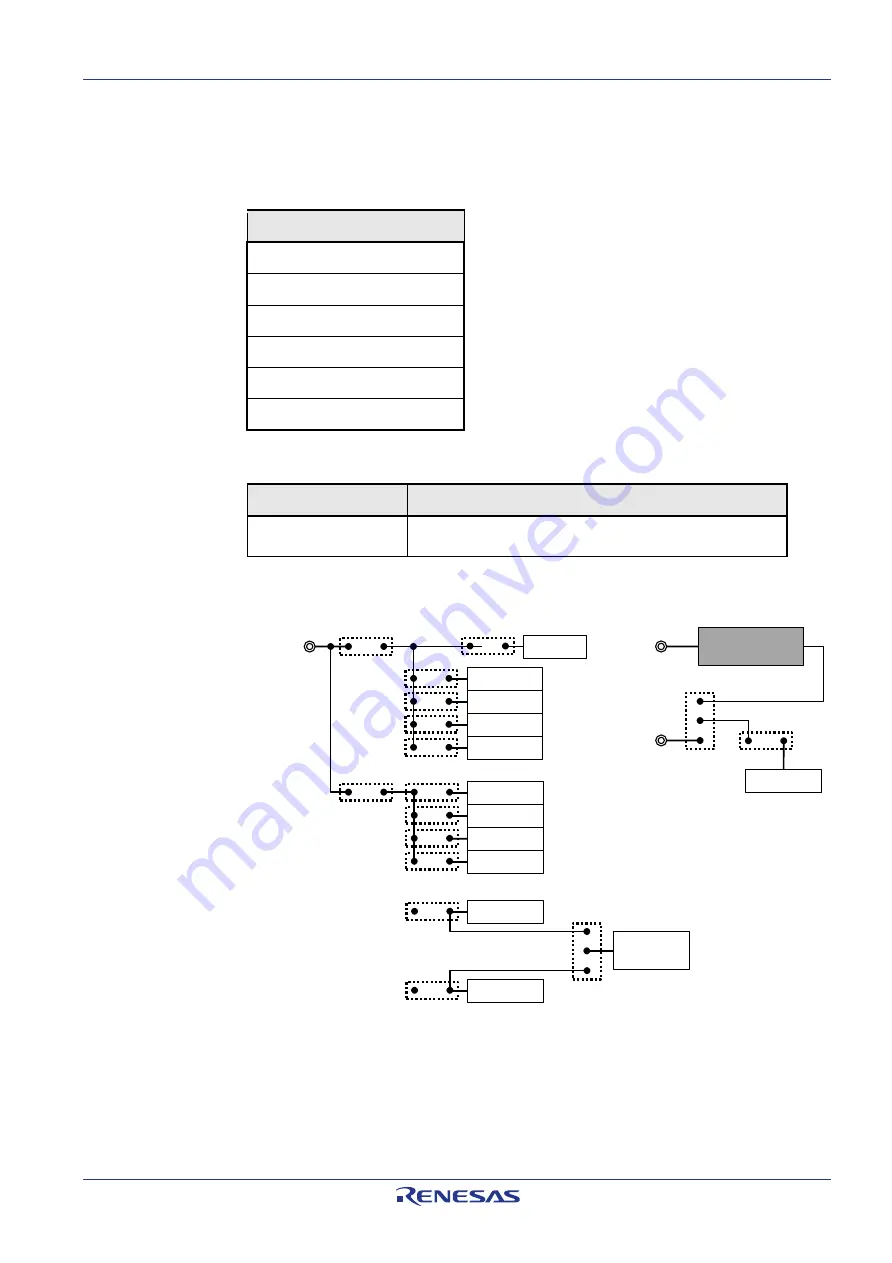
The following figure shows the configurable voltage distribution on the PiggyBack
board.
Figure 3 Voltage Distribution on the PiggyBack Board
All power supply lines can be interrupted by jumpers. This provides the
possibility to measure the current consumption of each individual power
domain of the device.
The IO supply voltage for the Mainboard (VDDIOF) can be connected via
jumper JP1 to
Voltage1
, if the PiggyBack board is mounted on a MainBoard.
VCC
A0VCC
Voltage regulator
for VDD
VDDIOF
E0VCC
JP0
SYSVCC
A0VREFH
E1VCC
A1VCC
A1VREFH
JP2
JP3
JP4
JP5
JP7
JP8
JP9
JP10
JP1
JP11
VCL/VDD
JP12
JP6
Voltage1
Voltage1
Voltage2
VCC
JP3
VCL/VDD
JP12
JP19
Pin 142
VCC/VDD
Содержание PiggyBack 144QFP
Страница 21: ...R20UT3282ED0101 Rev 1 1 21 2015 06 10 ...
Страница 22: ...R20UT3282ED0101 Rev 1 1 22 2015 06 10 ...
Страница 23: ...R20UT3282ED0101 Rev 1 1 23 2015 06 10 ...


