R-IN32M4-CL3 User's Manual: Board design edition
7. 2.5-V built-in Regulator Peripheral Circuit Configuration
R18UZ0074EJ0100
Page 23 of 61
Dec 24, 2019
7.5
Example of PCB Layout Image (23 mm Square BGA Package)
This section describes the peripheral circuit configuration of the 2.5-V built-in regulator installed in the R-IN32M4-CL3
in a 23 mm square BGA package.
7.5.1
L1 and L2 (23 mm Square BGA Package)
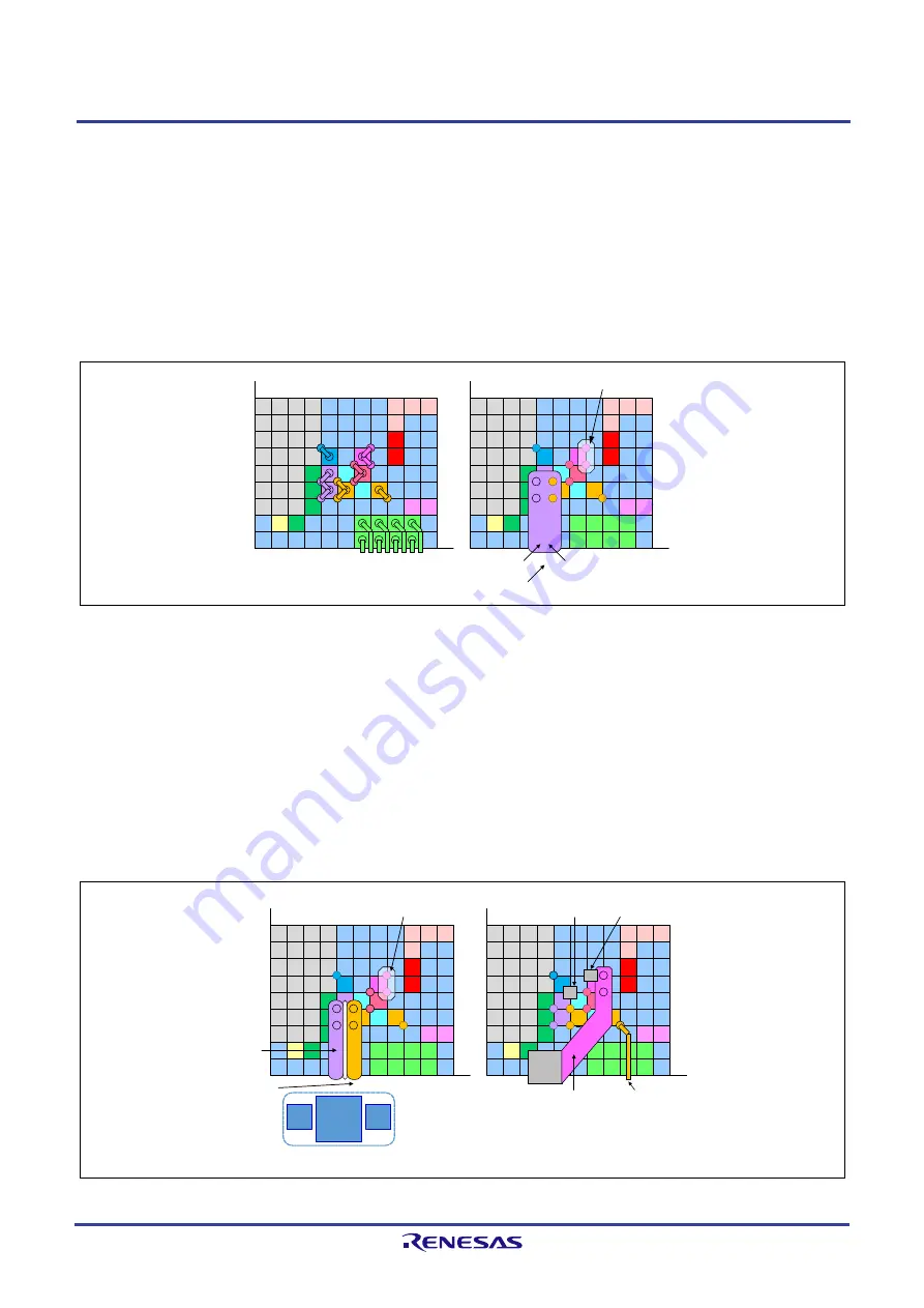
Followings are layout conditions and an example of PCB layout image (at the lower left of the L1 and L2).
Separate AGND of the built-in regulator from Digital GND as far as possible.
Do not pass through AGND under the MDI signal and the inductor component (L).
AGND
P0_
D0N
P0_
D0P
P0_
D1N
P0_
D1P
P0_
D2N
P0_
D2P
P0_
D3N
P0_
D3P
P0_
D0N
P0_
D0P
P0_
D1N
P0_
D1P
P0_
D2N
P0_
D2P
P0_
D3N
P0_
D3P
AVDD
REG_
33
AGND
REG_
FB
REG_
OUT
REG_
EN
VDD
REG_
33
AVDD
REG_
33
AGND
REG
_FB
REG_
OUT
REG_
EN
VDD
REG_
33
VDD
33
VDD
33
VDD
33
VDD
33
VDD
33
VDD
33
PCB L1
Connect to AGND of C
IN
and C
OUT
.
GND
GND
GND
GND
GND
GND
GND
GND/
OPEN
GND/
OPEN
GND/
OPEN
GND/
OPEN
GND
Do not pass AGND under the
MDI signal and the inductor
component (L).
VDD
11A
VDD
11A
VDD
11
VDD
33
VDD
11
VDD
11
VDD
33
VDD
11
VDD
11A
VDD
11A
Connect to GND at a single-point ground in front of this.
(In this case, do not use a ferrite bead.)
Removing the pattern
AGND
PCB L2 (GND)
Figure 7.3 Example of PCB Layout Image (L1 and L2) (23 mm Square BGA Package)
7.5.2
L3 and L4 (23 mm Square BGA Package)
Followings are layout conditions and an example of PCB layout image (at the lower left of the L3 and L4).
Place C
BYPASS
as close to the power supply pins (VDDREG_33 and AVDDREG_33).
Also, place L, C
IN
, and C
OUT
as close to the relevant pins as possible. In particular, placement of C
IN
is a high
priority.
Minimize the parasitic inductance of AVDDREG_33 pattern as small as possible.
The AVDDREG_33, AGND, and REG_OUT signals should be careful to avoid affecting other signals.
AGN
D
AGND
GND/
OPEN
P0_
D0N
P0_
D0P
P0_
D1N
P0_
D1P
P0_
D2N
P0_
D2P
P0_
D3N
P0_
D3P
P0_
D0N
P0_
D0P
P0_
D1N
P0_
D1P
P0_
D2N
P0_
D2P
P0_
D3N
P0_
D3P
AVDD
REG_3
3
AGND
REG_
FB
REG_
OUT
REG_
EN
VDD
REG_3
3
AVDD
REG_
33
AGND
REG_
FB
REG_
OUT
REG_
EN
VDD
REG_
33
VDD
33
VDD
33
VDD
33
VDD
33
VDD
33
VDD
33
VDD
11A
VDD
11A
GND/
OPEN
GND/
OPEN
GND/
OPEN
VDD
11
VDD
33
VDD
11
VDD
11A
VDD
11A
VDD
11
VDD
33
VDD
11
REG_
FB
Minimize parasitic inductance
to AVDDREG_33.
C
IN
C
BYPASS
REG_OUT
Place SBD, L, and C
OUT
compactly in front
of this to connect to the PCB.
Don't make an unnecessarily wide pattern
to avoid functioning as an antenna.
This pattern is a 2.5-V feedback voltage after smoothing with the
inductor (L) and capacitor (C
OUT
).
Keep away from the regulator related signals and the inductor (L).
Bypass capacitor for
AVDDREG_33
Connect to AGND
Bypass capacitor for
VDDREG_33
Connect to GND
L3 at this position, where L2 is AGND,
is preferably AGND than other power
sources.
Removing the pattern
AVDDREG_33
C
BYPASS
PCB L3 (VDD)
PCB L4
L
C
OUT
SBD
Place C
BYPASS
as close to the power supply pin (VDDREG_33 and AVDDREG_33).
Also, place C
IN
as close to the relevant pin as possible. (Placement of C
IN
is high priority
than that of SBD, inductor, and C
OUT
.)
Do not place C
IN
and C
OUT
side by side to prevent noise propagation.
SBD: Schottky Barrier Diode
Figure 7.4 Example of PCB Layout Image (L3 and L4) (23 mm Square BGA Package)


