HD74HCT1G04
Rev.5.00, Jan.28.2004, page 2 of 7
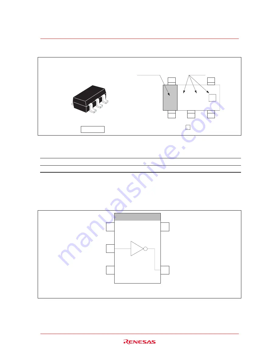
Outline and Article Indication
• HD74HCT1G04
Marking
= Control code
F 5
Index band
CMPAK–5
Function Table
Input A
Output
Y
H
L
L
H
H : High level
L : Low level
Pin Arrangement
(Top view)
5
4
V
CC
1
2
3
NC
IN Y
GND
OUT
Y


