


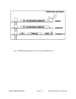


External I/O connections
Figure 2-3 shows the interface connector layout of the DM6854HR. This connector
is located toward the top of the board. Refer to this diagram when making isolated signal
output connections. Figure 2-4 shows the standard I/O connector pinout.
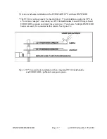
Figure 2-3a shows the screw terminal discrete wire connector pinout and figure 2-3b
shows the pinout of the same connector using a header connector.
Pin 1 is to the left side of the connector. ALL SIGNALS ARE ISOLATED
1.
IN1+
2.
IN1-
3.
IN2+
4.
IN2-
5.
IN3+
6.
IN3-
7.
IN4+
8.
IN4-
9.
IN5+
10.
IN5-
11.
IN6+
12.
IN6-
13.
IN7+
14.
IN7-
15.
IN8+
16.
IN8-
17.
OUT1_COLLECTOR
18.
OUT1_EMITTER
19.
OUT2_COLLECTOR
20.
OUT2_EMITTER
21.
OUT3_COLLECTOR
22.
OUT3_EMITTER
23.
OUT4_COLLECTOR
24.
OUT4_EMITTER
Fig. 2-3a Isolated Input/Output interface using screw terminal block connector
DM5854HR/DM6854HR Page 18 (c) RTD Finland Oy 1996-2001