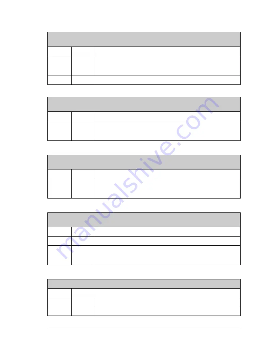
background image

Chapter 14  Timer B

119

Timer B Count MSB x Register

(TBM1R)

(Address = 0x00B2)

(TBM2R)

(Address = 0x00B4)

Bit(s)

Value

Description

7:6

Two MSBs of the compare value for the Timer B comparator. This compare 
value will be loaded into the actual comparator when the current compare detects 
a match.

5:0

These bits are reserved and should be written with zero.

Timer B Count LSB x Register

(TBL1R)

(Address = 0x00B3)

(TBL2R)

(Address = 0x00B5)

Bit(s)

Value

Description

7:0

Eight LSBs of the compare value for the Timer B comparator. This compare 
value will be loaded into the actual comparator when the current compare detects 
a match.

Timer B Step LSB x Register

(TBSL1R)

(Address = 0x00BA)

(TBSL2R)

(Address = 0x00BC)

Bit(s)

Value

Description

7:0

Eight LSBs of the step size for the Timer B comparator. The new compare value 
will be loaded into the actual comparator when the current compare detects a 
match.

Timer B Step MSB x Register

(TBSM1R)

(Address = 0x00BB)

(TBSM2R)

(Address = 0x00BD)

Bit(s)

Value

Description

7:2

These bits are ignored but should be written with zeros.

1:0

Two MSBs of the step size for the Timer B comparator. The new compare value 
will be loaded into the actual comparator when the current compare detects a 
match.

Timer B Count MSB Register

(TBCMR)

(Address = 0x00BE)

Bit(s)

Value

Description

7:6

read

The current value of the two MSBs of the Timer B counter are reported. 

5:0

These bits are always read as zeros.

Содержание Rabbit 4000

Страница 1: ...Rabbit 4000 Microprocessor User s Manual 019 0152 070720 H...

Страница 2: ...Semiconductor Inc Rabbit 4000 is a trademark of Rabbit Semiconductor Inc No part of the contents of this manual may be reproduced or transmitted in any form or by any means without the express writte...

Страница 3: ...ler 15 2 3 4 32 kHz Clock 18 2 4 Register Descriptions 20 Chapter 3 Reset and Bootstrap 25 3 1 Overview 25 3 1 1 Block Diagram 25 3 1 2 Registers 26 3 2 Dependencies 26 3 2 1 I O Pins 26 3 2 2 Clocks...

Страница 4: ...6 6 3 Interrupt Tables 66 Chapter 7 External Interrupts 69 7 1 Overview 69 7 2 Block Diagram 69 7 2 1 Registers 70 7 3 Dependencies 70 7 3 1 I O Pins 70 7 3 2 Clocks 70 7 3 3 Interrupts 70 7 4 Operati...

Страница 5: ...ort E 97 12 1 Overview 97 12 1 1 Block Diagram 99 12 1 2 Registers 100 12 2 Dependencies 100 12 2 1 I O Pins 100 12 2 2 Clocks 100 12 2 3 Other Registers 101 12 2 4 Interrupts 101 12 3 Operation 101 1...

Страница 6: ...pendencies 133 16 2 1 I O Pins 133 16 2 2 Clocks 134 16 2 3 Other Registers 134 16 2 4 Interrupts 134 16 3 Operation 135 16 3 1 Asynchronous Mode 135 16 3 2 Clocked Serial Mode 136 16 4 Register Descr...

Страница 7: ...er 182 19 3 5 2 Buffer Array 182 19 3 5 3 Linked List 183 19 3 5 4 Circular Queue 184 19 3 5 5 Linked Array 184 19 3 6 DMA with Peripherals 185 19 3 6 1 DMA with HDLC Serial Ports 185 19 3 6 2 DMA wit...

Страница 8: ...es 234 22 2 1 I O Pins 234 22 2 2 Clocks 234 22 2 3 Other Registers 234 22 2 4 Interrupts 234 22 3 Operation 235 22 3 1 Handling Interrupts 235 22 3 2 Example ISR 235 22 4 Register Descriptions 236 Ch...

Страница 9: ...scriptions 280 Chapter 27 System User Mode 283 27 1 Overview 283 27 1 1 Registers 284 27 2 Dependencies 285 27 2 1 I O Pins 285 27 2 2 Clocks 285 27 2 3 Other Registers 285 27 2 4 Interrupts 286 27 3...

Страница 10: ...Mechanical Dimensions and Land Pattern 322 29 2 Ball Grid Array Package 324 29 2 1 Pinout 324 29 2 2 Mechanical Dimensions and Land Pattern 325 29 3 Rabbit Pin Descriptions 327 Appendix A Parallel Por...

Страница 11: ...for up to 16 MB of memory Operating with a 1 8 V core and 3 3 or 1 8 V I O the Rabbit 4000 boasts an internal 10Base T Ethernet interface eight channels of DMA six serial ports with IrDA 40 digital I...

Страница 12: ...ble All six are configurable as asynchronous including output pulses in IrDA format while four are configurable as clocked serial SPI and two are configurable as SDLC HDLC The various internal periphe...

Страница 13: ...prying eyes The Rabbit 4000 has new peripherals DMA access and on chip Ethernet The Rabbit 4000 supports eight channels of DMA access to external memory internal I O addresses and the auxiliary I O bu...

Страница 14: ...TXA RXA CLKA ATXA ARXA TXB RXB CLKB ATXB ARXB TXC RXC CLKC TXD RXD CLKD ADDRESS BUS 15 bits RESOUT Asynch Serial Synch Serial Asynch Bootstrap Synch Bootstrap Serial Port A Asynch Serial IrDA Serial...

Страница 15: ...Maximum Clock Speed 60 MHz Digital I O 40 arranged in five 8 bit ports Serial Ports 6 CMOS compatible Ethernet Port 10Base T Baud Rate Clock speed 8 max asynchronous Address Bus 20 24 bit Data Bus 8...

Страница 16: ...8 100 Size of Package LQFP PQFP Spacing Between Package Pins 16 16 1 5 mm 0 4 mm 16 mils 16 16 1 5 mm 0 4 mm 16 mils 24 18 3 mm 0 65 mm 26 mils Size of Package TFBGA Spacing Between Package Pins 10 10...

Страница 17: ...IrDA Communication 6 6 None Serial Ports with Support for SDLC HDLC IrDA Communication 2 2 None Maximum Asynchronous Baud Rate Clock Speed 8 Clock Speed 8 Clock Speed 32 Ethernet Port 10Base T None No...

Страница 18: ...8 Rabbit 4000 Microprocessor User s Manual...

Страница 19: ...ons of the processor and separate power supply pins for the core and I O ring further reduce EMI from the Rabbit 4000 The main clock can be doubled or divided by 2 4 6 or 8 to reduce EMI and power con...

Страница 20: ...00000000 Global Clock Modulation 1 Register GCM1R 0x000B W 00000000 Global Clock Double Register GCDR 0x000F R W 00000000 NACR Ethernet Clock GCSR CPU Clock Peripheral Clock GOCR Divide by 2 CLK Pin...

Страница 21: ...in as well The peripheral clock or peripheral clock divided by 2 may be optionally output on the CLK pin by enabling it via bits 7 6 in GOCR The Ethernet clock may be input on pin PE6 by enabling it v...

Страница 22: ...PWM at their desired values When the 32 kHz clock is enabled in GCSR it can be further divided by 2 4 6 or 8 to generate even lower frequencies by enabling those modes in bits 0 2 of GPSCR See Table...

Страница 23: ...ifferently the maximum cycle shortening at 1 8 V and 25 C is shown in Table 2 2 below Table 2 2 Spectrum Spreader Settings 0 50 MHz 50 MHz GCM0R Value Description Max Cycle Shortening Normal 0x40 Norm...

Страница 24: ...ific manner with proper time delays GCM0R is only read by the spectrum spreader at the moment when the spectrum spreader is enabled by storing 0x080 in GCM1R If GCM1R is cleared when disabling the spe...

Страница 25: ...The clock doubler uses an on chip delay circuit that must be programmed by the user at startup if there is a need to double the clock Table 2 3 lists the recommended delays for the GCDR for various o...

Страница 26: ...created by xor ing the delayed and inverted clock with itself If the original clock does not have a 50 50 duty cycle then alternate clocks will have a slightly different length Since the duty cycle o...

Страница 27: ...n the falling edge of the clock are the mem ory and I O write pulses and the early option memory output enable See Chapter 5 for more information on the early output enable and write enable options Th...

Страница 28: ...s a very high imped ance making it susceptible to noise moisture and environmental contaminants It is strongly recommended to conformally coat this circuit to limit effects of temperature and humidity...

Страница 29: ...hort a time as possible when an ultra sleepy mode is enabled see Chapter 26 for more details on reducing power consumption When the 32 kHz clock is enabled the periodic interrupt is disabled automatic...

Страница 30: ...ock from the main clock 010 Processor clock from the main clock Peripheral clock from the main clock 011 Processor clock from the main clock divided by 2 Peripheral clock from the main clock divided b...

Страница 31: ...ther in 2 ns steps from 0 ns to 52 ns 11 This bit combination is reserved and must not be used 5 0 These bits are reserved and should be written with zeros Global Clock Modulator 1 Register GCM1R Addr...

Страница 32: ...time 00100 9 ns nominal low time 00101 10 ns nominal low time 00110 11 ns nominal low time 00111 12 ns nominal low time 01000 13 ns nominal low time 01001 14 ns nominal low time 01010 15 ns nominal lo...

Страница 33: ...byte fetch 01 STATUS pin is active low during an interrupt acknowledge 10 STATUS pin is low 11 STATUS pin is high 3 2 00 WDTOUT pin functions normally 01 Enable WDTOUT for test mode Rabbit Semiconduct...

Страница 34: ...are unused and should be written with zero 3 0 Normal operation 1 Restart auto negotiation process 2 0 Disable auto negotiation function 1 Enable auto negotiation function 1 0 Force half duplex operat...

Страница 35: ...e it either begins normal operation by fetching instruction bytes from CS0 and OE0 or it enters a special bootstrap mode where it fetches bytes from either Serial Port A or the slave port In this mode...

Страница 36: ...ep the RAM deselected during powerdown RESOUT The RESOUT pin is high during reset and powerdown but low at all other times and can be used to control an external power switch to disconnect VDDIO from...

Страница 37: ...trol an external power switch to disconnect VDDIO from VBATIO when the main power source is removed Table 3 1 lists the condition of the processor after reset takes place The state of all regis ters a...

Страница 38: ...t be disabled The device checks the state of the SMODE pins each time it jumps back to the start of the ROM program and responds according to the current state In addition by writing to bit 7 of the S...

Страница 39: ...010 Enable the slave port with SCS from Parallel Port E bit 7 011 Enable the auxiliary I O bus Parallel Port A is used for the data bus and Parallel Port B 7 2 is used for the address bus 100 This bit...

Страница 40: ...30 Rabbit 4000 Microprocessor User s Manual...

Страница 41: ...ithin that time Its purpose is to restart the processor when it detects that a program gets stuck or disabled The secondary watchdog timer can time out from 30 5 s up to 7 8 ms and generates a Priorit...

Страница 42: ...me Clock Byte 5 Register RTC5R 0x0007 R xxxxxxxx Watchdog Timer Control Register WDTCR 0x0008 W 00000000 Watchdog Timer Test Register WDTTR 0x0009 W 00000000 Secondary Watchdog Timer Register SWDTR 0x...

Страница 43: ...FEN pin can be active low during external I O cycles active low during data memory cycles or driven high or low The values in the battery backed onchip encryption RAM bytes are cleared If the signal o...

Страница 44: ...ld be read again Writing to RTC0R latches the current real time clock value into the RTCxR holding regis ters so the following sequence should be used to read the real time clock 1 Write any value to...

Страница 45: ...TCR The following steps explain how to use the secondary watchdog timer 1 Write the vector to the interrupt service routine to the internal interrupt table 2 Write the desired timeout period to SWDTR...

Страница 46: ...ck from the main clock 010 Processor clock from the main clock Peripheral clock from the main clock 011 Processor clock from the main clock divided by two Peripheral clock from the main clock divided...

Страница 47: ...ite 5 0 0 No effect on the real time clock counter 1 Increment the corresponding byte of the real time clock counter Real Time Clock x Register RTC0R Address 0x0002 RTC1R Address 0x0003 RTC2R Address...

Страница 48: ...nce of two writes where the first write is 0x51 0x52 or 0x53 followed by a write of 0x54 actually disables the watchdog timer The watchdog timer will be re enabled by any other write to this register...

Страница 49: ...This bit combination is reserved and should not be used 1 0 00 BUFEN pin is active low during external I O cycles 01 BUFEN pin is active low during data memory accesses 10 BUFEN pin is low 11 BUFEN pi...

Страница 50: ...oprocessor User s Manual Battery Backed Onchip Encryption RAM VRAM00 Address 0x0600 through through VRAM1F Address 0x061F Bit s Value Description 7 0 General purpose RAM locations Cleared by Intrusion...

Страница 51: ...orted The Rabbit 4000 s physical memory space contains four consecutive banks each of which can be mapped to an individual chip select enable strobe pair The banks can be set for equal sizes ranging f...

Страница 52: ...ace The boundaries between the root and data segments and the data and stack segments can be adjusted in 4KB blocks as well The XMEM segment is a fixed 8KB and points to a physical memory address spec...

Страница 53: ...ore bank selection physical device occurs These two features allow both code and data to access separate 64KB logical spaces instead of sharing a single space It is possible to protect memory in the R...

Страница 54: ...x MMU Expanded Code Register MECR 0x0018 R W 00000000 Memory Timing Control Register MTCR 0x0019 R W 00000000 Memory Alternate Control Register MACR 0x001D R W 00000000 Advanced CS0 Control Register A...

Страница 55: ...bit SRAM devices 5 2 2 Clocks All memory operations are clocked by the processor clock 5 2 3 Other Registers 5 2 4 Interrupts When a write is attempted to a write protected 64KB or 4KB block a write p...

Страница 56: ...e backwards compatibility to the Rabbit 2000 and 3000 processors these registers map directly to DATASEGL and STACKSEGL but the corresponding uppermost four bits are set to zero Each of these register...

Страница 57: ...valid setting before use The size of the memory banks can be defined in the MECR register The default size is 256KB the bank selection looks at address bits 18 and 19 but this value can be adjusted do...

Страница 58: ...is provides slightly longer strobes for slower memories see the timing diagrams in Chapter 28 These options are available in MTCR It is possible to force CS1 to be always active in MMIDR enabling this...

Страница 59: ...es are for those cases where a prefetch was started in anticipation of the queue being emptied The prefetch mechanism tracks the instructions being fetched and executed to minimize bus conflicts betwe...

Страница 60: ...ta is in the same page as the previous data In the Rabbit 4000 and most memory devices a page is 16 bytes Thus if an address is identical to the previous address except in the lower four bits the acce...

Страница 61: ...ce to operate in 16 bit mode This code is shown below This code should be the first thing executed by your device Because the processor is fetching bytes from a 16 bit memory device that is not connec...

Страница 62: ...ided into 4KB blocks by selecting them as the write protect segments A or B When a write is attempted to a block protected in WPxR WPSxLR or WPSxHR a Priority 3 write protect interrupt occurs This fea...

Страница 63: ...ct address MSB inversion for data accesses only This enables the instruction data split 4 0 Normal CS1 operation 1 Force CS1 always active This will not cause any conflicts as long as the memory using...

Страница 64: ...ical address offset to use if SEGSIZ 7 4 Addr 15 12 0xE Data Segment Register DATSEG Address 0x0012 Bit s Value Description 7 0 Read The current contents of this register are reported Write Eight LSBs...

Страница 65: ...es in this bank 11 Zero one for writes wait states for accesses in this bank 5 0 Pass bank select address MSB for accesses in this bank 1 Invert bank select address MSB for accesses in this bank 4 0 P...

Страница 66: ...B0CR independent of bank select address 101 For an XPC access use MB1CR independent of bank select address 110 For an XPC access use MB2CR independent of bank select address 111 For an XPC access use...

Страница 67: ...it states 3 0 Page mode operation disabled for CS1 1 Page mode operation enabled for CS1 Pages are 16 bytes Page mode accesses for program fetches only Use ACS1CR for wait states 2 1 00 Normal 8 bit o...

Страница 68: ...states for subsequent page mode accesses 11 Zero wait states for subsequent page mode accesses 2 0 000 Nine advanced or seven basic wait states for 16 bit bus write access 001 Eight advanced or six b...

Страница 69: ...t 59 Write Protection Control Register WPCR Address 0x0440 Bit s Value Description 7 1 These bits are reserved and should be written with zeros 0 0 Write protection in User Mode only 1 Write protectio...

Страница 70: ...isable write protection for the corresponding 64K segment 1 Enable write protection for the corresponding 64K block The 8 MSBs of the 24 bit physical address of any specific 64K block can be used to d...

Страница 71: ...for physical address 0x5000 0x5FFF in WP Segment x 1 Enable 4K write protect for physical address 0x5000 0x5FFF in WP Segment x 4 0 Disable 4K write protect for physical address 0x4000 0x4FFF in WP S...

Страница 72: ...00 0xBFFF in WP Segment x 1 Enable 4K write protect for physical address 0xB000 0xBFFF in WP Segment x 2 0 Disable 4K write protect for physical address 0xA000 0xAFFF in WP Segment x 1 Enable 4K write...

Страница 73: ...Register STKHLR Address 0x0446 Bit s Value Description 7 0 Upper limit for stack limit checking If a stack operation or stack relative memory access is attempted at an address greater than STKHLR 0xEF...

Страница 74: ...64 Rabbit 4000 Microprocessor User s Manual...

Страница 75: ...ny attempt to enter Priority 3 will actually be requested as Priority 2 When an interrupt is handled a call is executed to a fixed location in the interrupt vector tables this operation requires 10 cl...

Страница 76: ...er for more details 6 3 Interrupt Tables Table 6 1 shows the structure of the internal interrupt vector table The first column is the vector address offset within the table The second column shows the...

Страница 77: ...wn in Table 6 3 Interrupts marked as cleared automatically have their requests cleared when the inter rupt is first handled Table 6 2 External Interrupt Vector Table Structure Offset 0x0000 0x00 Exter...

Страница 78: ...from TCCSR Slave Port Rd Read from SPD0R SPD1R or SPD2R Wr Write to SPD0R SPD1R SPD2R or dummy write to SPSR DMA 7 Cleared automatically DMA 6 Cleared automatically DMA 5 Cleared automatically DMA 4 C...

Страница 79: ...upt pin must be present for at least three peripheral clock cycles to be detected In addition the Rabbit 4000 has a minimum latency of 10 clocks to respond to an interrupt so the minimum external inte...

Страница 80: ...IR at offsets 0x000 and 0x010 They can be set as Priority 1 2 or 3 in the appropriate IxCR 7 4 Operation The following steps must be taken to enable the external interrupts 1 Write the vector s to the...

Страница 81: ...nterrupt disabled 01 Parallel Port E high nibble interrupt on falling edge 10 Parallel Port E high nibble interrupt on rising edge 11 Parallel Port E high nibble interrupt on both edges 3 2 00 Paralle...

Страница 82: ...72 Rabbit 4000 Microprocessor User s Manual...

Страница 83: ...e SMODE pins have selected the slave port bootstrap mode Parallel Port A will be the slave port data bus until disabled by the processor Parallel Port A can also be used as an external I O data bus to...

Страница 84: ...ocked by the peripheral clock 8 2 3 Other Registers 8 2 4 Interrupts There are no interrupts associated with Parallel Port A 8 3 Operation The following steps explain how to set up Parallel Port A 1 S...

Страница 85: ...h zero 4 2 000 Disable the slave port Parallel Port A is a byte wide input port 001 Disable the slave port Parallel Port A is a byte wide output port 010 Enable the slave port with SCS from Parallel P...

Страница 86: ...76 Rabbit 4000 Microprocessor User s Manual...

Страница 87: ...carry the Slave Read strobe Slave Write strobe and Slave Address bits The Slave Chip Select can also be programmed to come from a Parallel Port B pin When the auxiliary I O bus option is enabled eith...

Страница 88: ...e Parallel Port B pins associated with those peripherals perform those actions no matter what the settings are in PBDR or PBDDR See the associated peripheral chapters for details on how they use Paral...

Страница 89: ...nformation Once the port is set up data can be read or written by accessing PBDR The value in PBDR of an output pin will reflect its current output value but any value written to an input pin will not...

Страница 90: ...le the slave port with SCS from Parallel Port E bit 7 011 Enable the auxiliary I O bus Parallel Port A is used for the data bus and Parallel Port B 7 2 is used for the address bus 100 This bit combina...

Страница 91: ...be used as inputs to various on chip peripherals Table 10 1 Parallel Port C Pin Alternate Output Functions Pin Name Alt Out 0 Alt Out 1 Alt Out 2 Alt Out 3 PC7 TXA I7 PWM3 SCLKC PC6 TXA I6 PWM2 TXE PC...

Страница 92: ...an output the value it is set to is returned 10 1 1 Block Diagram 10 1 2 Registers Register Name Mnemonic I O Address R W Reset Port C Data Register PCDR 0x0050 R W 00010101 Port C Data Direction Reg...

Страница 93: ...eripheral clock 10 2 3 Other Registers 10 2 4 Interrupts There are no interrupts associated with Parallel Port C 10 3 Operation The following steps must be taken before using Parallel Port C 1 Select...

Страница 94: ...Description 7 6 00 Parallel Port C bit 3 alternate output 0 TXC 01 Parallel Port C bit 3 alternate output 1 I3 10 Parallel Port C bit 3 alternate output 2 TIMER C3 11 Parallel Port C bit 3 alternate...

Страница 95: ...arallel Port C bit 5 alternate output 1 I5 10 Parallel Port C bit 5 alternate output 2 PWM1 11 Parallel Port C bit 5 alternate output 3 RCLKE 1 0 00 Parallel Port C bit 4 alternate output 0 TXB 01 Par...

Страница 96: ...86 Rabbit 4000 Microprocessor User s Manual...

Страница 97: ...ield to control this timing Each bit can either be programmed as open drain or driven high and low Because of the buffered nature of Parallel Port D using a read modify write type of oper ation can le...

Страница 98: ...rt D Pin Alternate Input Functions Pin Name Input Capture Serial Ports A D Serial Ports E F DMA External Interrupts Quad Decode PD7 RXA RXE PD6 PD5 RXB RCLKE PD4 TCLKE PD3 RXC RXF DREQ1 QRD2A PD2 SCLK...

Страница 99: ...xR Data 7 0 7 0 External I O Strobes Serial Ports A F Tx Rx Clocks 7 0 7 0 7 5 3 1 PWM Output Timer C Output Input Capture 3 0 7 5 3 1 Quadrature Decoder 3 0 7 4 External I O Address 7 6 16 bit Data B...

Страница 100: ...D are clocked by the peripheral clock unless changed in PDCR where the option of updating the Parallel Port D pins can be synchronized to the output of Timer A1 Timer B1 or Timer B2 Register Name Mne...

Страница 101: ...be superseded if a 16 bit memory interface is selected since par allel port D is used for the upper half of the data bus in that mode Once Parallel Port D is set up data can be read or written by acce...

Страница 102: ...3 alternate output 1 I3 10 Parallel Port D bit 3 alternate output 2 TIMER C3 11 Parallel Port D bit 3 alternate output 3 SCLKD 5 4 00 Parallel Port D bit 2 alternate output 0 SCLKC 01 Parallel Port D...

Страница 103: ...KE 1 0 00 Parallel Port D bit 4 alternate output 0 TXB 01 Parallel Port D bit 4 alternate output 1 I4 10 Parallel Port D bit 4 alternate output 2 PWM0 11 Parallel Port D bit 4 alternate output 3 TCLKE...

Страница 104: ...ister PDDDR Address 0x0067 Bit s Value Description 7 0 0 The corresponding port bit is input 1 The corresponding port bit is an output Parallel Port D Bit 0 Register PDB0R Address 0x0068 Bit s Value D...

Страница 105: ...it The port buffer will be transferred to the port output register on the next rising edge of the peripheral clock Parallel Port D Bit 4 Register PDB4R Address 0x006C Bit s Value Description 7 5 3 0 T...

Страница 106: ...f this bit The port buffer will be transferred to the port output register on the next rising edge of the peripheral clock Parallel Port D Bit 7 Register PDB7R Address 0x006F Bit s Value Description 6...

Страница 107: ...f the port having a separate select field to control this timing Each bit can either be programmed as open drain or driven high and low Because of the buffered nature of Parallel Port E using a read m...

Страница 108: ...Input Functions Pin Name Input Capture Serial Ports A D Serial Ports E F DMA External Interrupts Quad Decode Ethernet PE7 RXA RXE DREQ1 PE6 DREQ0 ECLK PE5 RXB RCLKE INT1 PE4 TCLKE INT0 PE3 RXC RXF DR...

Страница 109: ...PEDR PEBxR Data 7 0 7 0 Ethernet Clock and LEDs Serial Ports A F Tx Rx Clocks 7 0 7 5 4 0 PWM Output Timer C Output Input Capture 3 0 7 5 3 1 Quadrature Decoder 3 0 7 4 A0 A 23 20 External I O Strobes...

Страница 110: ...Clocks All outputs on Parallel Port E are clocked by the peripheral clock unless changed in PECR where the option of updating the Parallel Port E pins can be synchronized to the output of Timer A1 Tim...

Страница 111: ...er for further use of that pin Once the port is set up data can be read or written by accessing PEDR The value of an output pin read in from PEDR will reflect its current output value but any value wr...

Страница 112: ...t 3 alternate output 1 A23 10 Parallel Port E bit 3 alternate output 2 TIMER C3 11 Parallel Port E bit 3 alternate output 3 SCLKD 5 4 00 Parallel Port E bit 2 alternate output 0 I2 01 Parallel Port E...

Страница 113: ...alternate output 3 RCLKE 1 0 00 Parallel Port E bit 4 alternate output 0 I4 01 Parallel Port E bit 4 alternate output 1 A0 10 Parallel Port E bit 4 alternate output 2 PWM0 11 Parallel Port E bit 4 al...

Страница 114: ...gister PEDDR Address 0x0077 Bit s Value Description 7 0 0 The corresponding port bit is input 1 The corresponding port bit is an output Parallel Port E Bit 0 Register PEB0R Address 0x0078 Bit s Value...

Страница 115: ...bit The port buffer will be transferred to the port output register on the next rising edge of the peripheral clock Parallel Port E Bit 4 Register PEB4R Address 0x007C Bit s Value Description 7 5 3 0...

Страница 116: ...of this bit The port buffer will be transferred to the port output register on the next rising edge of the peripheral clock Parallel Port E Bit 7 Register PEB7R Address 0x007F Bit s Value Description...

Страница 117: ...can be programmed to generate an interrupt Six of these seven timers A2 A7 have the option of being cascaded from Timer A1 but the primary clock for all of the timers is the periph eral clock either...

Страница 118: ...ete If a bit is on and the corresponding interrupt is enabled an interrupt will occur when priorities allow However a separate interrupt is not guaranteed for each bit with an enabled interrupt If the...

Страница 119: ...TACR perclk 2 Timer A2 Timer A7 Parallel Ports D E Control Timer B Timer C Input Capture PWM Quadrature Decoder Timer A8 Timer A9 Timer A10 Serial Ports A F Interrupt Generation Output TACR TACSR TAT...

Страница 120: ...Status Register TACSR 0x00A0 R W 00000000 Timer A Prescale Register TAPR 0x00A1 R W xxxxxxx1 Timer A Time Constant 1 Register TAT1R 0x00A3 R W xxxxxxxx Timer A Control Register TACR 0x00A4 R W 0000000...

Страница 121: ...able Timer A by writing a 1 to bit 0 of TACSR 13 3 1 Handling Interrupts The following steps explain how an interrupt is set up and used Remember to set up the interrrupt vector before you enable the...

Страница 122: ...its are cleared by the read of this register as is the Timer A interrupt 7 1 0 The corresponding Timer A interrupt is disabled Write only 1 The corresponding Timer A interrupt is enabled 0 0 The main...

Страница 123: ...r A1 2 0 Timer A2 clocked by the main Timer A clock 1 Timer A2 clocked by the output of Timer A1 1 0 00 Timer A interrupts are disabled 01 Timer A interrupt use Interrupt Priority 1 10 Timer A interru...

Страница 124: ...or clock from the main clock divided by two Peripheral clock from the main clock divided by two 100 Processor clock from the 32 kHz clock optionally divided via GPSCR Peripheral clock from the 32 kHz...

Страница 125: ...B can clock the outputs on Parallel Ports D and E The compare value comes from either the match register or the value internally generated via the step register When using the match register a new ma...

Страница 126: ...is cleared when TBCSR is read Register Name Mnemonic I O Address R W Reset Timer B Control Status Register TBCSR 0x00B0 R W xxxx0000 Timer B Control Register TBCR 0x00B1 R W xx000000 Timer B MSB 1 Reg...

Страница 127: ...et up and used 1 Write the vector to the interrupt service routine to the internal interrupt table 2 Configure TBCSR to select which match registers will generate an interrupt 3 Configure TBCR to sele...

Страница 128: ...1 The main clock for Timer B the peripheral clock divided by 2 is enabled Timer B Control Register TBCR Address 0x00B1 Bit s Value Description 7 6 These bits are reserved and should be written with z...

Страница 129: ...detects a match Timer B Step LSB x Register TBSL1R Address 0x00BA TBSL2R Address 0x00BC Bit s Value Description 7 0 Eight LSBs of the step size for the Timer B comparator The new compare value will be...

Страница 130: ...or clock from the main clock Peripheral clock from the main clock 011 Processor clock from the main clock divided by two Peripheral clock from the main clock divided by two 100 Processor clock from th...

Страница 131: ...counter is reloaded with zeros allowing the con trol registers to be reloaded at any time during the count cycle Timer C can generate an interrupt when the count limit value is reached A separate Tim...

Страница 132: ...essor User s Manual 15 1 1 Block Diagram Timer C TCCR perclk 2 perclk 16 Timer A1 Interrupt Generation Interrupt Request Up Counter Divider Registers Timer Cx RESET set x Register reset x Register Set...

Страница 133: ...er TCS1LR 0x050C R W xxxxxxxx Timer C Set 1 High Register TCS1HR 0x050D R W xxxxxxxx Timer C Reset 1 Low Register TCR1LR 0x050E R W xxxxxxxx Timer C Reset 1 High Register TCR1HR 0x050F R W xxxxxxxx Ti...

Страница 134: ...peripheral clock divided by 2 by the peripheral clock divided by 16 or by the output of timer A1 as selected in TCCR 15 2 3 Other Registers 15 2 4 Interrupts A Timer C interrupt is enabled in TCCR and...

Страница 135: ...TCBPR 5 Enable the desired output pins for Timer C by writing to the appropriate parallel port function and alternate output registers 6 Enable Timer C by writing a 1 to bit 0 of TCCSR 15 3 1 Handling...

Страница 136: ...0501 Bit s Value Description 7 4 These bits are reserved and should be written with zero 3 2 00 Timer C clocked by the peripheral clock divided by 2 01 Timer C clocked by the output of Timer A1 10 Tim...

Страница 137: ...x Timer C Reset x Low Register TCR0LR Address 0x050A TCR1LR Address 0x050E TCR2LR Address 0x051A TCR3LR Address 0x051E Bit s Value Description 7 0 Eight LSBs of the match value to reset Timer C Output...

Страница 138: ...in clock 010 Processor clock from the main clock Peripheral clock from the main clock 011 Processor clock from the main clock divided by two Peripheral clock from the main clock divided by two 100 Pro...

Страница 139: ...a byte may be read while another byte is being received or the next byte to be transmitted can be loaded while the current byte is still being transferred out The byte is available in the buffer after...

Страница 140: ...ks can be generated from the appropriate 8 bit timer from Timer A shown in Table 16 1 or from a dedicated n 1 15 bit divider In either case the resulting byte data rate in the asynchronous mode is 1 8...

Страница 141: ...e break or charac ter assembly can be inhibited to reduce the interrupt overhead 16 1 1 Block Diagram Serial Ports A D Peripheral Clock Serial Port Control 15 bit Divider Timer Ax Output Tx Pins SxDHR...

Страница 142: ...ister SBER 0x00D5 R W 00000000 Serial Port B Divider Low Register SBDLR 0x00D6 R W xxxxxxxx Serial Port B Divider High Register SBDHR 0x00D7 R W 0xxxxxxx Serial Port C Data Register SCDR 0x00E0 R W xx...

Страница 143: ...t C is used as a clocked serial port and 8 bit memories are used the serial clock is transmitted on PD2 and so PD2 will not be available for other use Serial Port D can transmit on parallel port pins...

Страница 144: ...ceive buffer or when a byte is finished being transmitted out of the transmit buffer The serial port interrupt vectors are located in the IIR as follows Serial Port A at offset 0x0C0 Serial Port B at...

Страница 145: ...clock polarity and behavior during break 5 Write the desired divider value to TATxR for the appropriate serial port or else write a divider value to the dedicated 15 bit divider in SxDLR and SxDHR If...

Страница 146: ...e Also select the interrupt priority 4 Select additional options by writing to SxER clock polarity bit order and clock source if external 5 Write the desired divider value to TATxR for the appropriate...

Страница 147: ...z check_for_tx rx_ready ioi ld a SADR read byte and clear interrupt do something with received byte here ld a 0x41 set bits 6 7 to 01 the other bits should represent the desired SACR setup ioi ld SACR...

Страница 148: ...n the clocked serial mode automatically causes the receiver to start a byte receive operation eliminating the need for software to issue the start receive command Write Loads the transmit buffer with...

Страница 149: ...he receive buffer was not overrun 1 The receive buffer was overrun This bit is cleared by reading the receive buffer 4 0 The byte in the receive buffer has no parity error or was not checked for parit...

Страница 150: ...er was overrun This bit is cleared by reading the receive buffer 4 0 This bit is always zero in the clocked serial mode 3 0 The transmit buffer is empty 1 The transmit buffer is not empty The serial p...

Страница 151: ...peration simultaneously 5 4 00 Parallel Port C is used for input 01 Parallel Port D is used for input 10 Parallel Port E is used for input 11 Disable the receiver input 3 2 00 Asynchronous mode with 8...

Страница 152: ...nd checking with space always zero parity 111 Enable parity generation and checking with mark always one parity 4 0 Normal asynchronous data encoding 1 Enable RZI coding 3 16 bit cell IrDA compliant 3...

Страница 153: ...l clock 11 Inverted clocked serial clock polarity inactive high Internal clock only 3 0 Normal bit order LSB first for transmit and receive 1 Reverse bit order MSB first for transmit and receive 2 0 S...

Страница 154: ...0x00F7 Bit s Value Description 7 0 Disable the serial port divider and use the output of Timer A to clock the serial port 1 Enable the serial port divider and use its output to clock the serial port T...

Страница 155: ...nformation on whether a received byte is available the receive buffer was over run a parity error was received and the transmit buffer is empty or busy sending a byte The status is updated when the fi...

Страница 156: ...ck rate divided by 16 When using an external clock a 1 same speed as the data rate clock is supported In this case the maximum data rate is 1 6 of the peripheral clock rate The receive clock is gener...

Страница 157: ...EER 0x00CD R W 00000000 Serial Port E Divider Low Register SEDLR 0x00CE R W xxxxxxxx Serial Port E Divider High Register SEDHR 0x00CF R W 0xxxxxxx Serial Port F Data Register SFDR 0x00D8 R W xxxxxxxx...

Страница 158: ...C0 PD0 or PE0 while the receive serial clock is either transmitted or received on PC1 PD1 or PE1 17 2 2 Clocks The data clocks for Serial Ports E F are based on the peripheral clock and divided by eit...

Страница 159: ...mit buffer In the HDLC mode interrupts are also generated by the reception of an end of frame with abort valid CRC or CRC error at the end of a transmission of a CRC by an abort sequence or by a closi...

Страница 160: ...n behavior and combined or separate clocks 5 Write the desired divider value to TATxR for the appropriate serial port or else write a divider to the dedicated 15 bit divider in SxDLR and SxDHR If the...

Страница 161: ...o SEAR or SELR instead ioi ld SEDR a load next byte into buffer and clear interrupt done pop af ipres ret 17 3 3 More on Clock Synchronization and Data Encoding The transmitter is not capable of sendi...

Страница 162: ...transitions on the receive data stream to adjust its count The DPLL adjusts the count so that the DPLL output will be properly placed in the bit cells to sample the receive data To work properly then...

Страница 163: ...are present in the receive data stream Two consecu tive missed transitions causes the DPLL to halt operation and wait for the next available transition This mode of operation is necessary because it...

Страница 164: ...lock transition at the center of every bit cell and optional data transitions occur at the bit cell boundaries The DPLL only uses the clock transitions to track the bit cell boundaries by ignoring all...

Страница 165: ...Address 0x00C8 SFDR Address 0x00D8 Bit s Value Description 7 0 Read Returns the contents of the receive buffer Write Loads the transmit buffer with a data byte for transmission Serial Port x Address...

Страница 166: ...fer was not overrun 1 The receive buffer was overrun This bit is cleared by reading the receive buffer 4 0 The byte in the receive buffer has no parity error or was not checked for parity 1 The byte i...

Страница 167: ...uffer is not empty The serial port will request an interrupt when the transmitter takes a byte from the transmit buffer unless the byte is marked as the last in the frame Transmit interrupts are clear...

Страница 168: ...eceiver data input Clocks from Parallel Port E 3 2 00 Asynchronous mode with 8 bits per character 01 Asynchronous mode with 7 bits per character In this mode the most significant bit of a byte is igno...

Страница 169: ...ays zero parity 111 Enable parity generation and checking with mark always one parity 4 0 Normal asynchronous data encoding 1 Enable RZI coding 3 16 bit cell IrDA compliant 3 0 Normal break operation...

Страница 170: ...nsmit flag on underrun 1 Transmit abort on underrun 1 0 Separate HDLC external receive and transmit clocks 1 Combined HDLC external and transmit clock from transmit clock pin 0 This bit is ignored in...

Страница 171: ...nput or data output register to indicate the empty or full status of the data register Data registers are marked full when written by the source side of the interface and are marked empty when read by...

Страница 172: ...c I O Address R W Reset Slave Port Data 0 Register SPD0R 0x0020 R W xxxxxxxx Slave Port Data 1 Register SPD1R 0x0021 R W xxxxxxxx Slave Port Data 2 Register SPD2R 0x0022 R W xxxxxxxx Slave Port Status...

Страница 173: ...r the master writes to SPD0R The SLVATTN pin is asserted whenever the slave device writes to SPD0R Either if these conditions is cleared when either the master or slave reads or writes any of the slav...

Страница 174: ...lave port connection between a Rabbit processor as the master and two slaves Figure 18 1 Master Slave Port Connections MASTER Rabbit First SLAVE Rabbit Second SLAVE Rabbit D0 D7 IORD IOWR A0 A1 CLK PE...

Страница 175: ...ange on SLVATTN it reads the slave port data registers 18 3 1 Master Setup 1 Enable the I O strobes on PD6 and PD7 by writing to the appropriate Parallel Port D pin and external I O registers 2 Enable...

Страница 176: ...t is writing multiple bytes SPD0R should be written last which enables the SLVATTN line 2 The master receives an external interrupt from the SLVATTN line and reads the data out of the slave port data...

Страница 177: ...guration is useful when fewer signals are desired or the master device has no external interrupts available If polling is to be used it is important to note that not all bits in the status register ma...

Страница 178: ...master reads writes the slave port registers Figure 18 2 Slave Port R W Timing Diagram SCS SD 7 0 SRD Slave Port Read Cycle Slave Port Write Cycle SWR SA1 SA0 Tsu SCS Tsu SA Th SA Th SCS Tw SRD Ten S...

Страница 179: ...CS SCS Hold Time 0 Tsu SA SA Setup Time 5 Th SA SA Hold Time 0 Tw SRD SRD Low Pulse Width 40 Ten SRD SRD to SD Enable Time 0 Ta SRD SRD to SD Access Time 30 Tdis SRD SRD to SD Disable Time 15 Tsu SRW...

Страница 180: ...s Value Description 7 0 Processor wrote to SPSR 1 Master wrote to Data Register 0 6 0 Slave port read byte 2 is empty 1 Slave port read byte 2 is full 5 0 Slave port read byte 1 is empty 1 Slave port...

Страница 181: ...ave port with SCS from Parallel Port E bit 7 011 Enable the auxiliary I O bus Parallel Port A is used for the data bus and Parallel Port B 7 2 is used for the address bus 100 This bit combination is r...

Страница 182: ...172 Rabbit 4000 Microprocessor User s Manual...

Страница 183: ...ly as a function of the internal I O address loaded into the DMA channel Note that if both the source and the destination are internal I O the source transfer request is used by the DMA channel The DM...

Страница 184: ...d in the buffer descriptor DMA memory addresses are always physical addresses and are never translated by the MMU All DMA memory addresses use the memory control signals wait states and flipped bits a...

Страница 185: ...t in Ethernet peripheral is used it is expected that two DMA channels will be dedicated for that purpose 19 1 1 Block Diagram Interrupt Generation Peripheral Clock Interrupt Request DMA DMRxCR DMCR Ex...

Страница 186: ...r Unused 7 0 Register DyBU0R 0x01yA R 00000000 DMA y Buffer Unused 15 8 Register DyBU1R 0x01yB R 00000000 DMA y Initial Address 7 0 Register DyIA0R 0x01yC R W xxxxxxxx DMA y Initial Address 15 8 Regis...

Страница 187: ...operations If the timed request option is enabled then the 16 bit timed request counter will be clocked by the peripheral clock and will provide a DMA request each time it counts down to zero 19 2 3 I...

Страница 188: ...ps explain how to set up a DMA channel 1 Select the DMA transfer and interrupt priorities by writing to DMCR 2 Select the DMA channel priority maximum bytes per burst and minimum clocks between bursts...

Страница 189: ...MA is active This includes handling interrupts so it is important to limit the amount of time that the DMA can operate This is handled in several ways First of all the DMA transfers can be set to take...

Страница 190: ...transfers and consists of one instruction fetch time plus three clock cycles The byte fetched during the instruction fetch time is discarded and will be refetched at the completion of the DMA burst At...

Страница 191: ...byte transferred and if a higher priority channel has a pending request the current transfer will be terminated and the new channel transfer will start The other option is to rotate after every burst...

Страница 192: ...can also generate interrupts The advantage of the buffer array is that its descriptors require less memory than a full 16 byte descriptor The simplest version of the buffer array is a double buffer w...

Страница 193: ...descriptors are not necessarily adjacent in memory The advantage of this mode is the ability to spread descriptors Buffer Descriptor 12 bytes Initial Address Linked List Interrupt Buffer Descriptor 16...

Страница 194: ...buffer while the other buffer is being loaded 19 3 5 5 Linked Array The linked array is simply a linked list of buffer arrays where the last buffer in each array is linked to the first buffer in the...

Страница 195: ...R the final byte of the transfer will be written to the last data register NALDR as required to complete an Ethernet packet and append the CRC value In addition the value in the network status registe...

Страница 196: ...s when execution is rewound after the DMA transfer The result of this mismatch is that the block copy instruction does not complete The only way to prevent this from occurring is to prevent DMA transf...

Страница 197: ...y 1 The corresponding DMA channel is enabled and active These bits are set by the start command and remain set until the completion of the last buffer DMA Master Auto Load Register DMALR Address 0x010...

Страница 198: ...This feature is intended only for testing because the DMA automatically resets the counter to all ones when fetching from the initial address The counter is incremented whenever the DMA fetches a new...

Страница 199: ...after the current channel request is serviced 5 3 000 Maximum one byte per burst 001 Maximum two bytes per burst 010 Maximum three bytes per burst 011 Maximum four bytes per burst 100 Maximum eight b...

Страница 200: ...sfer per request 01 External DMA Request 0 rising edge triggered One transfer per request 10 External DMA Request 0 active low Transfers continue while low 11 External DMA Request 0 active high Transf...

Страница 201: ...equest 01 External DMA Request 1 rising edge triggered One transfer per request 10 External DMA Request 1 active low Transfers continue while low 11 External DMA Request 1 active high Transfers contin...

Страница 202: ...be used 2 0 000 Timed DMA request supplied to DMA Channel 0 001 Timed DMA request supplied to DMA Channel 1 010 Timed DMA request supplied to DMA Channel 2 011 Timed DMA request supplied to DMA Chann...

Страница 203: ...be used in the compare to generate the termination condition A zero in a bit position disables the corresponding bit from contributing to the termination condition A value of all zeros in this registe...

Страница 204: ...R Address 0x016C D7IA0R Address 0x017C Bit s Value Description 7 0 Bits 7 0 of the initial address are stored in this register DMA y Initial Addr 15 8 Register D0IA1R Address 0x010D D1IA1R Address 0x0...

Страница 205: ...ng Byte Count 0 next 11110010 Fetching Byte Count 1 next 11101110 Fetching Source Address 0 next 11101100 Fetching Source Address 1 next 11101010 Fetching Source Address 2 next 11011110 Fetching Desti...

Страница 206: ...s long 5 0 No special treatment for last byte 1 Internal Source status byte written to initial buffer descriptor before last data Internal Destination Last byte written to offset address for frame ter...

Страница 207: ...uffer length value are stored in this register The DMA does a transfer followed by a decrement of this register so an initial value of 0x0000 will result in a 65536 byte transfer DMA y Length 15 8 Reg...

Страница 208: ...ter D0SA1R Address 0x0185 D1SA1R Address 0x0195 D2SA1R Address 0x01A5 D3SA1R Address 0x01B5 D4SA1R Address 0x01C5 D5SA1R Address 0x01D5 D6SA1R Address 0x01E5 D7SA1R Address 0x01F5 Bit s Value Descript...

Страница 209: ...1R Address 0x0189 D1DA1R Address 0x0199 D2DA1R Address 0x01A9 D3DA1R Address 0x01B9 D4DA1R Address 0x01C9 D5DA1R Address 0x01D9 D6DA1R Address 0x01E9 D7DA1R Address 0x01F9 Bit s Value Description 7 0...

Страница 210: ...ster D0LA1R Address 0x018D D1LA1R Address 0x019D D2LA1R Address 0x01AD D3LA1R Address 0x01BD D4LA1R Address 0x01CD D5LA1R Address 0x01DD D6LA1R Address 0x01ED D7LA1R Address 0x01FD Bit s Value Descrip...

Страница 211: ...etried up to 16 times using the standard random back off time algorithm Detection of a collision causes the transmitter to send a 32 bit jam pattern of all ones to guarantee that all receivers in the...

Страница 212: ...add The first received byte adds to the lower byte of the checksum and the second received byte adds to the upper byte of the checksum In the case of a frame with an odd length the second received by...

Страница 213: ...e Section 20 4 for more details 20 1 1 Block Diagram 10Base T Network Port Network Port Control TxD TxDD TxD TxDD Network Receiver Multicast Filter NAMHR NAMExR Network Port Status Network Transmitter...

Страница 214: ...ort A Phys Addr 31 24 Register NAPA3R 0x0213 W xxxxxxxx Network Port A Phys Addr 39 32 Register NAPA4R 0x0214 W xxxxxxxx Network Port A Phys Addr 47 40 Register NAPA5R 0x0215 W xxxxxxxx Network Port A...

Страница 215: ...ource this clock from the processor clock or the processor clock divided by two assuming a 20 MHz or a 40 MHz clock is installed If the processor clock is used the clock doubler and dither should be d...

Страница 216: ...memory and write it to NADR Write the buffer descriptor s address to the DMA s initial address registers see Chapter 19 for more information 2 Enable the DMA transfer by auto loading the buffer 3 The...

Страница 217: ...nsmit error occur jp nz handle_tx_err pop af bit 2 a did link change or jabber occur ioi ld a NASR get current status to check which one bit 0 a jp nz handle_jabber did jabber condition occur done pop...

Страница 218: ...r program control A one in the corresponding table entry con stitutes a multicast address match as far as the network port is concerned A table of one set of unique multicast addresses corresponding t...

Страница 219: ...2 3 4 SN65LVDS2 10 nF 470 W 10 nF 3 3 V 100 W 1 kW 1 kW RxD 3 3 V 10 nF 1 5 2 3 4 SN65LVDS2 RxD 2 2 kW 2 2 kW 82 5 W 10 nF 270 pF 270 pF 220 pF 820 nH 820 nH 10 nF 220 pF TxD TxDD TxD TxDD 110 W 110 W...

Страница 220: ...ORd with NAPCR 6 to provide level inversion Network Port A Data Register NADR Address 0x0200 Bit s Value Description 7 0 Read Returns the contents of the receive buffer This register is not normally a...

Страница 221: ...NARSR Address 0x0203 Bit s Value Description 7 4 0000 Receiver is disabled or has not yet received a frame after being enabled 0xx1 Frame discarded because of FIFO overrun during reception The missed...

Страница 222: ...memory buffer space is reclaimed 5 0 Frame transmission not complete Read only 1 Frame transmitted without error 4 0 No error on frame transmission Read only 1 Frame transmission aborted because of e...

Страница 223: ...clear this condition Network Port A Reset Register NARR Address 0x0206 Bit s Value Description 7 0 No operation 1 Reset the network port transmitter This command clears the jabber condition and purge...

Страница 224: ...are unused and should be written with zero 3 0 Normal operation 1 Restart auto negotiation process 2 0 Disable auto negotiation function 1 Enable auto negotiation function 1 0 Force half duplex opera...

Страница 225: ...valid signal qualifier RXD is XORd with NAPCR 7 and RXD is XORd with NAPCR 6 to provide level inversion 4 0 These bits are unused and should be written with zeros Network Port A Pin Control Register...

Страница 226: ...ll 5 0 Normal receiver operation 1 Place receiver in Monitor mode Receiver operates normally but does not buffer frames to memory 4 0 Receive frames less than 64 bytes in length discarded 1 Receive fr...

Страница 227: ...ite Eight bits of the multicast filter At the end of a received multicast address the upper six bits of CRC are used as an index into this 64 bit table If the corresponding bit is zero the frame is di...

Страница 228: ...urned This counter is cleared by a read of this register Network Port A Checksum 0 Register NAC0R Address 0x0224 Bit s Value Description 7 0 read The LSB of the checksum for the completed frame is ret...

Страница 229: ...output of Timer A8 and can be set to count at a rate ranging from the full clock speed perclk 2 down to 1 256 the clock speed perclk 512 Two events are recognized a start condition and a stop conditio...

Страница 230: ...cesses the capture event and set up the output pulse synchronized by Timer B The minimum time delay needed is prob ably less than 10 s if the software is done carefully and the clock speed is reasonab...

Страница 231: ...r 1 Register ICT1R 0x0058 R W 00000000 Input Capture Source 1 Register ICS1R 0x0059 R W xxxxxxxx Input Capture LSB 1 Register ICL1R 0x005A R xxxxxxxx Input Capture MSB 1 Register ICM1R 0x005B R xxxxxx...

Страница 232: ...pts Each input capture channel can generate an interrupt whenever a start stop condition occurs or when the counter rolls over to zero The interrupt request is cleared when ICCSR is read The input cap...

Страница 233: ...nerate an interrupt 3 Configure the Input Capture Control Register ICCR to select the interrupt priority note that interrupts will be enabled once this value is set this step should be done last The f...

Страница 234: ...Software Start to an External Event The following steps explain how to measure the time interval between a software start and the occurrence of an external event 1 Set up the counter to run continuou...

Страница 235: ...ead 1 The Input Capture 2 counter has rolled over to all zeros 2 0 The Input Capture 1 counter has not rolled over to all zeros Read 1 The Input Capture 1 counter has rolled over to all zeros 7 2 Read...

Страница 236: ...operation for Input Capture 2 6 0 Input Capture operation for Input Capture 1 1 Input Count operation for Input Capture 1 5 2 These bits are reserved and should be written with zero 1 0 00 Input Captu...

Страница 237: ...urn the programmed match value 01 Latch the count on the Stop condition only 10 Latch the count on the Start condition only 11 Latch the count on either the Start or Stop condition 3 2 00 Ignore the s...

Страница 238: ...p condition input 10 Parallel Port E used for Stop condition input 11 This bit combination is reserved and should not be used 1 0 00 Use port bit 1 for Stop condition input 01 Use port bit 3 for Stop...

Страница 239: ...0x005F Bit s Value Description 7 0 Read The most significant eight bits of the latched Input capture count are returned In Counter operation if no latching condition is specified the value written to...

Страница 240: ...230 Rabbit 4000 Microprocessor User s Manual...

Страница 241: ...nputs to pre vent false counts The external signals are synchronized with an internal clock provided by the output of Timer A10 Each Quadrature Decoder channel accepts inputs from either the upper nib...

Страница 242: ...t clock cycles Input capture may be used to measure the pulse width on the I inputs because they come from the odd numbered port bits The operation of the digital filter is shown below The Quadrature...

Страница 243: ...0x0091 R W 00000000 Quad Decode Count 1 Register QDC1R 0x0094 R xxxxxxxx Quad Decode Count 1 High Register QDC1HR 0x0095 R xxxxxxxx Quad Decode Count 2 Register QDC2R 0x0096 R xxxxxxxx Quad Decode Co...

Страница 244: ...0R The clock rate must be high enough that transitions on the inputs are sampled in different clock cycles In addition both the I and Q inputs go through a digital filter that rejects pulses shorter t...

Страница 245: ...ote that interrupts will be enabled once this value is set The following actions occur within the interrupt service routine Since a Quadrature Decoder interrupt occurs when the counter rolls over dete...

Страница 246: ...ead of this register 5 This bit always reads as zero 4 0 No effect on the Quadrature Decoder 2 Write only 1 Reset Quadrature Decoder 2 to all zeros without causing an interrupt 3 0 Quadrature Decoder...

Страница 247: ...se Quadrature Decoder 1 to increment or decrement 01 Quadrature Decoder 1 inputs from Parallel Port D bits 1 and 0 10 Quadrature Decoder 1 inputs from Parallel Port E bits 1 and 0 11 Quadrature Decode...

Страница 248: ...238 Rabbit 4000 Microprocessor User s Manual...

Страница 249: ...o reduce rip ple on the externally filtered PWM output The PWM outputs can be passed through a fil ter and used as a 10 bit D A converter The outputs can also be used to directly drive devices such as...

Страница 250: ...Rabbit 4000 are designed to work with fixed I O addresses To allow DMA control of the PWM a separate PWM Block Access Register PWBAR and PWM Block Pointer Register PWBPR are available The pointer regi...

Страница 251: ...0R 0x0088 R W xxxxx00x PWM MSB 0 Register PWM0R 0x0089 R W xxxxxxxx PWM LSB 1 Register PWL1R 0x008A R W xxxxx00x PWM MSB 1 Register PWM1R 0x008B R W xxxxxxxx PWM LSB 2 Register PWL2R 0x008C R W xxxxx0...

Страница 252: ...sters 23 2 4 Interrupts The PWM can generate an interrupt for every PWM counter rollover every second roll over every fourth rollover or every eighth rollover This option is selected in PWL1R The inte...

Страница 253: ...rupt is set up and used 1 Write the vector to the interrupt service routine to the internal interrupt table 2 Configure PWL0R to select the PWM interrupt priority and PWL1R to select PWM interrupt sup...

Страница 254: ...Width Modulator interrupts use Interrupt Priority 3 0 0 PWM output High for single block 1 Spread PWM output throughout the cycle PWM LSB 1 Register PWL1R Address 0x008A Bit s Value Description 7 6 Le...

Страница 255: ...oughout the cycle PWM MSB x Register PWM0R Address 0x0089 PWM1R Address 0x008B PWM2R Address 0x008D PWM3R Address 0x008F Bit s Value Description 7 0 Most significant eight bits for the Pulse Width Mod...

Страница 256: ...246 Rabbit 4000 Microprocessor User s Manual...

Страница 257: ...l I O transaction until the external device is ready to complete the transac tion A timeout period can be defined to ensure that the processor is not held indefinitely by a misbehaving external device...

Страница 258: ...on the memory bus alone or both buses It is also possible to shorten the read strobe by one clock cycle and the write strobe by one half a clock cycle by pulling in the trailing edge which guarantees...

Страница 259: ...d cannot accept a transaction The Rabbit 4000 will then hold midway through the transaction until either the handshake signal goes inactive or a timeout occurs The timeout can be defined anywhere from...

Страница 260: ...r IB2CR 0x0082 W 00000000 I O Bank 3 Control Register IB3CR 0x0083 W 00000000 I O Bank 4 Control Register IB4CR 0x0084 W 00000000 I O Bank 5 Control Register IB5CR 0x0085 W 00000000 I O Bank 6 Control...

Страница 261: ...lel Ports C D or E each bank can be directed to the appropriate pin bank zero on PC0 PD0 or PE0 bank one on PC1 PD1 or PE1 etc The strobes will affect outputs on IOWR IORD and BUFEN at all times The I...

Страница 262: ...eps must be taken before using an I O strobe 1 Set the strobe type and timing for a particular device by writing to the appropriate IBxCR register for the I O bank desired 2 If signals other than IORD...

Страница 263: ...tive high I O transaction held until signal goes low 3 This bit is reserved and should be written with zero 2 0 000 Use Parallel Port E bit 0 for I O handshake 001 Use Parallel Port E bit 1 for I O ha...

Страница 264: ...le I O handshake for I O Bank 2 1 0 Disable I O handshake for I O Bank 1 1 Enable I O handshake for I O Bank 1 0 0 Disable I O handshake for I O Bank 0 1 Enable I O handshake for I O Bank 0 I O Handsh...

Страница 265: ...ignal is an I O chip select 01 The I signal is an I O read strobe 10 The I signal is an I O write strobe 11 The I signal is an I O data read or write strobe 3 0 Writes are not allowed to this bank Tra...

Страница 266: ...ble the slave port with SCS from Parallel Port E bit 7 011 Enable the auxiliary I O bus Parallel Port A is used for the data bus and Parallel Port B 7 2 is used for the address bus 100 This bit combin...

Страница 267: ...tput 0 TXC 01 Parallel Port C bit 2 alternate output 1 I2 10 Parallel Port C bit 2 alternate output 2 TIMER C2 11 Parallel Port C bit 2 alternate output 3 TXF 3 2 00 Parallel Port C bit 1 alternate ou...

Страница 268: ...2 PWM2 11 Parallel Port C bit 6 alternate output 3 TXE 3 2 00 Parallel Port C bit 5 alternate output 0 TXB 01 Parallel Port C bit 5 alternate output 1 I5 10 Parallel Port C bit 5 alternate output 2 P...

Страница 269: ...ut 0 SCLKC 01 Parallel Port D bit 2 alternate output 1 I2 10 Parallel Port D bit 2 alternate output 2 TIMER C2 11 Parallel Port D bit 2 alternate output 3 TXF 3 2 00 Parallel Port D bit 1 alternate ou...

Страница 270: ...2 PWM2 11 Parallel Port D bit 6 alternate output 3 TXE 3 2 00 Parallel Port D bit 5 alternate output 0 IA6 01 Parallel Port D bit 5 alternate output 1 I5 10 Parallel Port D bit 5 alternate output 2 P...

Страница 271: ...tput 0 I2 01 Parallel Port E bit 2 alternate output 1 A22 10 Parallel Port E bit 2 alternate output 2 TIMER C2 11 Parallel Port E bit 2 alternate output 3 TXF 3 2 00 Parallel Port E bit 1 alternate ou...

Страница 272: ...PWM2 11 Parallel Port E bit 6 alternate output 3 TXE 3 2 00 Parallel Port E bit 5 alternate output 0 I5 01 Parallel Port E bit 5 alternate output 1 LINK 10 Parallel Port E bit 5 alternate output 2 PW...

Страница 273: ...ill not yet be enabled at the end of that instruction and the interrupt will instead occur at the end of the next instruction Note that a breakpoint may be forced to be pending by setting the correspo...

Страница 274: ...essor User s Manual 25 1 1 Block Diagram Address Compare Interrupt Request Breakpoint x BxCR BxM0R BxM1R BxM2R BxA0R BxA1R BxA2R Code Execution Data Read Data Write Address Interrupt Generation Addres...

Страница 275: ...0000 Breakpoint 1 Address 0 2 Register B1AxR 0x031C x R W 00000000 Breakpoint 2 Address 0 2 Register B2AxR 0x032C x R W 00000000 Breakpoint 3 Address 0 2 Register B3AxR 0x033C x R W 00000000 Breakpoin...

Страница 276: ...irst 25 3 Operation The following steps must be taken to enable breakpoints 1 Write the vector to the interrupt service routine to the external interrupt table 2 Write the desired breakpoint addresses...

Страница 277: ...low breakpoint_isr push af ioi ld a BDCR determine which interrupts are pending and clear the interrupt request handle all breakpoints here reenable any breakpoints by writing to BDCR pop af ipres you...

Страница 278: ...ress 0x033B B4CR Address 0x034B B5CR Address 0x036B B6CR Address 0x037B Bit s Value Description 7 6 00 No Breakpoint x on execute address match 01 Breakpoint x on User Mode execute address match 10 Br...

Страница 279: ...kpoint x Address 1 Register B0A1R Address 0x030D B1A1R Address 0x031D B2A1R Address 0x032D B3A1R Address 0x033D B4A1R Address 0x034D B5A1R Address 0x036D B6A1R Address 0x037D Bit s Value Description 7...

Страница 280: ...B0M1R Address 0x0309 B1M1R Address 0x0319 B2M1R Address 0x0329 B3M1R Address 0x0339 B4M1R Address 0x0349 B5M1R Address 0x0369 B6M1R Address 0x0379 Bit s Value Description 7 0 Breakpoint x Mask 15 8 A...

Страница 281: ...y modes various shortened chip select strobes are available to reduce current draw by the attached memory devices Figure 26 1 shows a typical current draw as a function of the main clock frequency The...

Страница 282: ...r the Ultra Sleepy Modes 26 1 1 Registers Register Name Mnemonic I O Address R W Reset Global Control Status Register GCSR 0x0000 R W 11000000 Global Power Save Control Register GPSCR 0x000D R W 00000...

Страница 283: ...y 8 with the peripheral clock at full speed If the clock doubler is enabled the options also include twice the main oscillator frequency and the main oscillator divided by 3 In addition the 32 kHz clo...

Страница 284: ...idth of the chip select the power consumption of the memory chip can be reduced without having any affect on the processor itself For reduced processor speeds based on the main oscillator a short chip...

Страница 285: ...Chapter 26 Low Power Operation 275 CLK1 CLK A 23 0 D 7 0 CSx OEx valid T1 T2 Divide by 6 Mode CLK1 CLK A 23 0 D 7 0 CSx OEx valid T1 T2 Divide by 4 Mode...

Страница 286: ...e chip select signal that is the width of a single 32 kHz clock 30 5 microseconds oth erwise the timing is identical to the short chip select options based off the main oscillator Read strobe figures...

Страница 287: ...Chapter 26 Low Power Operation 277 32 kHz CLK A 23 0 D 7 0 CSx OEx valid T1 T2 Operation at 4 kHz 32 kHz CLK A 23 0 D 7 0 CSx OEx valid T1 T2 Operation at 8 kHz...

Страница 288: ...278 Rabbit 4000 Microprocessor User s Manual 32 kHz CLK A 23 0 D 7 0 CSx OEx valid T1 T2 Operation at 16 kHz 32 kHz CLK A 23 0 D 7 0 CSx OEx valid T1 T2 Operation at 32 kHz...

Страница 289: ...via GPSCR to reduce power consumption even more when running off the 32kHz oscillator When self timed chip selects are enabled the chip select is only active for a short selectable period of time A s...

Страница 290: ...lock from the fats clock 010 Processor clock from the fast clock Peripheral clock from the fast clock 011 Processor clock from the fast clock divided by 2 Peripheral clock from the fast clock divided...

Страница 291: ...11 110 ns self timed chip selects for read only 4 0 Normal chip select timing for read cycles 1 Short chip select timing for read cycles not available in full speed 3 0 Normal chip select timing for w...

Страница 292: ...time 00100 9 ns nominal low time 00101 10 ns nominal low time 00110 11 ns nominal low time 00111 12 ns nominal low time 01000 13 ns nominal low time 01001 14 ns nominal low time 01010 15 ns nominal lo...

Страница 293: ...the processor s I O registers and preventing memory writes to critical regions the user s code can run without the danger of locking up the processor to the point where it cannot be restarted remotel...

Страница 294: ...ter ICUER 0x0358 W 00000000 I O Bank User Enable Register IBUER 0x0380 W 00000000 PWM User Enable Register PWUER 0x0388 W 00000000 Quad Decode User Enable Register QDUER 0x0390 W 00000000 External Int...

Страница 295: ...dulator 1 Register GCM1R 0x000B Secondary Watchdog Timer Register SWDTR 0x000C Global Power Save Control Register GPSCR 0x000D Global Output Control Register GOCR 0x000E Global Clock Double Register G...

Страница 296: ...stem User Mode is enabled and the pro cessor is in the User Mode If the processor is placed into Priority 3 either by an instruc tion or an interrupt it will respond as if it was set to Priority 2 Whe...

Страница 297: ...pts to be used are set up for the User Mode critical memory regions are protected stack limits are set and the various system memory stack violation interrupts are enabled The processor then enters th...

Страница 298: ...pheral and or interrupt from the System Mode If allowed the System Mode can create an interrupt vector as described in Section 27 3 7 that will execute the user code interrupt handler When the applica...

Страница 299: ...ss 2 Write a 1 to bit 0 of EDMR to enable System User Mode 3 Execute the SETUSR instruction to enter User Mode After the User Mode is entered the limitations described earlier are in effect writes to...

Страница 300: ...ser Mode or an interrupt occurs or SYSCALL or RST is executed to enter System Mode the current mode is pushed onto the SU register When a SURES is executed the previous mode is popped off the SU regis...

Страница 301: ...t vectors to the same address as SYSCALL The difference is that it also pushes the value of the SU register as well as the return address onto the stack SRET is the companion instruction to SCALL it e...

Страница 302: ...Mode before calling the User Mode interrupt handler An example of both system and user interrupt handling is shown in Figure 27 4 When enabled for User Mode access a peripheral interrupt if it is capa...

Страница 303: ...e_isr jumped to from interrupt vector table handle interrupt sures reenter previous mode ipres restore previous interrupt priority ret usermode_isr jumped to from interrupt vector table still in syste...

Страница 304: ...Enable Register PAUER Address 0x0330 Bit s Value Description 7 0 Disable User Mode access to Parallel Port A I O addresses 0x0030 0x0037 1 Enable User Mode access to Parallel Port A I O addresses 0x00...

Страница 305: ...Register PEUER Address 0x0370 Bit s Value Description 7 0 Disable User Mode access to Parallel Port E I O addresses 0x0070 0x007F 1 Enable User Mode access to Parallel Port E I O addresses 0x0070 0x0...

Страница 306: ...0x0083 2 0 Disable User Mode access to I O Bank 2 and internal I O address 0x0082 1 Enable User Mode access to I O Bank 2 and internal I O addresses 0x0082 1 0 Disable User Mode access to I O Bank 1...

Страница 307: ...er Mode access to Timer A I O addresses 0x00A0 0x00AF 1 Enable User Mode access to Timer A I O addresses 0x00A0 0x00AF 6 0 These bits are reserved and should be written with zeros Timer B User Enable...

Страница 308: ...nable Register SCUER Address 0x03E0 Bit s Value Description 7 0 Disable User Mode access to Serial Port C I O addresses 0x00E0 0x00E7 1 Enable User Mode access to Serial Port C I O addresses 0x00E0 0x...

Страница 309: ...These bits are reserved and should be written with zeros Enable Dual Mode Register EDMR Address 0x0420 Bit s Value Description 7 6 00 Default Rabbit 2000 3000 instruction set 01 This bit combination i...

Страница 310: ...300 Rabbit 4000 Microprocessor User s Manual...

Страница 311: ...MHz 25 C 3 7 mA Core current 32 768 kHz 25 C 22 A I O Ring I O Ring Supply Voltage 3 3 V VDDIO 3 0 V 3 3 V 3 6 V I O Ring Supply Voltage 1 8 V 1 65 V 1 8 V 1 90 V I O Ring Current 29 4912 MHz 3 3 V 2...

Страница 312: ...10 VDDIO 3 3V 10 TA 40 C to 85 C Parameter Symbol Min Typ Max VBAT VBAT Supply Voltage VBAT 1 65 V 1 8 V 1 90 V VBAT Current device powered down IVBAT 1 7 A 2 7 A VBATIO VBATIO Supply Voltage device p...

Страница 313: ...8 3 Preliminary AC Electrical Characteristics VDDCORE 1 8 V 10 VDDIO 3 3 V 10 TA 40 C to 85 C Parameter Symbol Min Typ Max Main Clock Frequency on CLKI fmain 60 MHz Real Time Clock Frequency on CLK32K...

Страница 314: ...y Memory Read Time Delays VDDCORE 1 8 V 10 VDDIO 3 3 V 10 TA 40 C to 85 C Parameter Symbol Loading Min Typ Max Clock to Address Delay Tadr 30 pF 6 ns 60 pF 8 ns 90 pF 11 ns Clock to Memory Chip Select...

Страница 315: ...yp Max Clock to Address Delay Tadr 30 pF 6 ns 60 pF 8 ns 90 pF 11 ns Clock to Memory Chip Select Delay TCSx 30 pF 6 ns 60 pF 8 ns 90 pF 11 ns Clock to Memory Write Strobe Delay TWEx 30 pF 6 ns 60 pF 8...

Страница 316: ...1 Memory Read and Write Cycles Tadr Tadr Memory Read no wait states CLK A 19 0 Memory Write no extra wait states CLK A 19 0 valid T1 T2 T1 Tw T2 valid TOEx TOEx D 7 0 valid Thold Tsetup CSx OEx TCSx T...

Страница 317: ...Early Output Enable and Write Enable Timing Tadr Tadr Memory Read no wait states CLK A 19 0 Memory Write no extra wait states CLK A 19 0 valid T1 T2 T1 Tw T2 valid TOEx TOEx D 7 0 valid Thold Tsetup...

Страница 318: ...x Clock to Address Delay Tadr 30 pF 6 ns 60 pF 8 ns 90 pF 11 ns Clock to Memory Chip Select Delay TCSx 30 pF 6 ns 60 pF 8 ns 90 pF 11 ns Clock to I O Chip Select Delay TIOCSx 30 pF 6 ns 60 pF 8 ns 90...

Страница 319: ...ns Clock to Memory Chip Select Delay TCSx 30 pF 6 ns 60 pF 8 ns 90 pF 11 ns Clock to I O Chip Select Delay TIOCSx 30 pF 6 ns 60 pF 8 ns 90 pF 11 ns Clock to I O Write Strobe Delay TIOWR 30 pF 6 ns 60...

Страница 320: ...fault or active high Tadr Tadr External I O Read no extra wait states CLK A 15 0 External I O Write no extra wait states CLK A 15 0 IORD valid T1 Tw T1 Tw T2 valid T2 BUFEN IOCSx IOWR BUFEN D 7 0 vali...

Страница 321: ...of wait states is used then the memory access time will be affected slightly When the clock spectrum spreader is enabled clock periods are shortened by a small amount depending on whether the normal o...

Страница 322: ...the high part of the clock If the doubler is not enabled then every clock is shortened during the low part of the clock period The maximum shortening for a pair of clocks combined is shown in the tabl...

Страница 323: ...ation should be considered When the doubler is enabled 80 of the nominal value should be used for the memory access time calculation clock 29 49 MHz so T 34 ns operating voltage is 3 3 V the clock dou...

Страница 324: ...l specifications preliminary The commercial rating calls for a 5 voltage variation from 3 3 V and a temperature range from 40 to 70 C The industrial ratings stretch the voltage variation to 10 over a...

Страница 325: ...that it not be less than 2 ns Thus 3 ns must be added to the minimum period of 21 ns giving a minimum period of 24 ns and a maximum frequency of 41 6 MHz commercial Table 28 11 Preliminary Maximum Clo...

Страница 326: ...duty cycle to obtain the highest clock speeds using the clock doubler you must use an external oscillator buffer that will allow for duty cycle adjustment by changing the resistance of the power and g...

Страница 327: ...duce current consumption the clock can be divided down in one of the sleepy modes see Table 26 1 for more details Figure 28 5 shows a typical current draw as a function of the main clock frequency The...

Страница 328: ...he low frequencies possible in the ultra sleepy modes as low as 2 kHz the external memory devices become signifi cant factors in the current consumption unless one of the short or self timed chip sele...

Страница 329: ...unning at 3 3 V normally A circuit to switch between a 1 8 2 0 V battery and the main power can use the RESOUT pin to switch the power source for the VBATIO pin R is a current limiting resistor that s...

Страница 330: ...320 Rabbit 4000 Microprocessor User s Manual...

Страница 331: ...118 117 116 115 114 113 112 111 110 109 108 107 106 105 104 103 102 101 100 99 98 97 VSSIO A19 OE1 A11 A9 A8 VDDINT VSSINT A13 A14 VDDIO VSSIO A17 WE0 A18 A16 A15 A12 A7 A6 VDDIO VSSIO A5 A4 VDDINT VS...

Страница 332: ...d Pattern Figure 29 2 Mechanical Dimensions Rabbit LQFP Package 14 00 0 10 mm 16 00 0 25 mm 0 10 mm 0 15 mm 0 60 0 18 0 05 mm 0 40 mm 14 00 0 10 mm 16 00 0 25 mm 1 00 mm The same pin dimensions apply...

Страница 333: ...IL 1999 Figure 29 3 PC Board Land Pattern for Rabbit 4000 128 pin LQFP 13 75 mm min 16 85 mm max 12 4 mm 15 3 mm 0 28 mm max 0 40 mm 13 75 mm min 16 85 mm max 12 4 mm 15 3 mm 1 55 mm JT 0 29 0 55 mm T...

Страница 334: ...PA3 PA0 WE1 STATUS OE0 A10 VDDIO VSSIO PB4 PB0 CLKI PA5 VDDIO VSSIO A19 VDDINT VSSINT CS0 D7 PB7 PB3 VDDIO VSSIO OE1 A11 A9 A8 VSSIO VDDIO D6 D5 A14 A13 VSSINT VDDINT D4 D3 D2 D1 VDDIO VSSIO A17 WE0 A...

Страница 335: ...ns and Land Pattern Figure 29 5 BGA Package Outline A B C D E F G H J K L M 12 11 10 9 8 7 6 5 4 3 2 1 A B C D E F G H J K L M 12 11 10 9 8 7 6 5 4 3 2 1 0 80 10 00 0 05 0 80 10 00 0 05 0 20 0 30 1 20...

Страница 336: ...Ball Pitch mm Nominal Land Diameter mm Land Variation mm 0 3 0 35 0 25 0 8 0 25 0 25 0 20 Table 29 2 Design Considerations all dimensions in mm Key Feature Recommendation A Solder Land Diameter 0 254...

Страница 337: ...g Timer Timeout 41 L4 STATUS Output Instruction Fetch First Byte 4 C1 SMODE1 SMODE0 Input Bootstrap Mode Tamper Detect 42 43 M4 J5 Chip Selects CS0 Output Memory Chip Select 0 9 D3 CS1 Output Memory C...

Страница 338: ...or User s Manual Network TXD TXD TXDD TXDD Output Network Transmit 124 127 B3 B4 A4 A3 RXD RXD Input Network Receive 121 122 A5 A5 Table 29 3 Rabbit 4000 Pin Descriptions Pin Group Pin Name Direction...

Страница 339: ...T PINS WITH ALTERNATE FUNCTIONS A 1 Alternate Parallel Port Pin Outputs Table A 1 Alternate Parallel Port A and B Pin Outputs Pin Alternate Output Options Serial Clock I O Mode Slave Mode PA 7 0 Data...

Страница 340: ...8 PE7 I7 ACT PWM3 SCLKC PE6 I6 PWM2 TXE PE5 I5 LINK PWM1 RCLKE PE4 I4 A0 PWM0 TCLKE PE3 I3 A23 TIMER C3 SCLKD PE2 I2 A22 TIMER C2 TXF PE1 I1 A21 TIMER C1 RCLKF PE0 I0 A20 TIMER C0 TCLKF When Serial Po...

Страница 341: ...orts A D Serial Ports E F PA 7 0 Data PB7 PB6 SCS PB5 SA1 PB4 SA0 PB3 SRD PB2 SWR PB1 SCLKA PB0 SCLKB PC7 Yes RXA RXE PC6 PC5 Yes RXB RCLKE PC4 TCLKE PC3 Yes RXC RXF PC2 PC1 Yes RXD RCLKF PC0 TCLKF PD...

Страница 342: ...QRD2A RXC RXF PE2 DREQ0 Yes QRD2B SCLKC PE1 Yes INT1 Yes QRD1A RXD RCLKF PE0 INT0 Yes QRD1B SCLKD TCLKF Table A 3 Alternate Parallel Port Pin Inputs continued Pin Input Capture DMA External Interrupt...

Страница 343: ...ds 333 APPENDIX B RABBIT 4000 ESD DESIGN GUIDELINES AND BUG WORKAROUNDS The Rabbit 4000 began shipping in 2006 and has undergone one minor respin since that time Several bugs were found in the design...

Страница 344: ...itional protection AT58206 UL2T LQFP AT58206 JCT2T TFBGA NOTE All Rabbit processors are sensitive to ESD and should be handled appropriately B 1 1 ESD Design Guidelines The following design guidelines...

Страница 345: ...s logical address limits 3 DMA HDLC Ethernet interaction a specific bug can manifest itself when the following conditions are present The HDLC or Ethernet peripherals are being fed bytes for transmit...

Страница 346: ...and set to transfer a single byte at a time to an internal I O register two bytes will actually be transferred The simplest workaround is to double each data byte in the buffer two bytes will be tran...

Страница 347: ...way to avoid the bug is to increase the number of wait states if possible on the device operating in the basic mode Using this option will produce a loss of performance Finally this bug is best avoide...

Страница 348: ...338 Rabbit 4000 Microprocessor User s Manual...

Страница 349: ...gs workarounds 335 advanced 16 bit mode 336 DMA requests to internal I O registers 186 336 DMA block copy interaction 186 336 DMA HDLC Ethernet interaction 185 335 stack protection DMA interaction 35...

Страница 350: ...cies 70 example ISR 70 interrupt vectors 70 operation 70 register descriptions 71 registers 70 input capture channels 222 223 example ISR 223 internal interrupt vector table 66 interrupt priorities 68...

Страница 351: ...setup 87 register descriptions 92 registers 90 Parallel Port E 97 alternate input functions 98 alternate output functions 97 block diagram 99 clocks 100 dependencies 100 interrupts 101 operation 101...

Страница 352: ...14 120 128 280 GOCR 23 39 GPSCR 281 GREV 39 IBUER 296 ICCR 226 ICCSR 225 ICLxR 228 ICMxR 229 ICSxR 228 ICTxR 227 ICUER 295 IHCR 253 IHSR 254 IHTR 254 IOxCR 255 IUER 297 IxCR 71 MACR 57 MBxCR 55 MECR 5...

Страница 353: ...269 Breakpoint x Control Register 268 Breakpoint x Mask 0 Register 270 Breakpoint x Mask 1 Register 270 Breakpoint x Mask 2 Register 270 Breakpoint Debug Control Register 268 clocks 10 Global Clock Do...

Страница 354: ...ol Register 58 DataSegmentHighRegister 54 Data Segment Low Register 54 Data Segment Register 54 Memory Alternate Control Register 57 Memory Bank x Control Register 55 Memory Timing Control Register 56...

Страница 355: ...5 Parallel Port E Bit 6 Register 106 Parallel Port E Bit 7 Register 106 Parallel Port E Control Register 103 Parallel Port E Data Direction Register 104 Parallel Port E Data Register 102 Parallel Port...

Страница 356: ...7 Timer B User Enable Register 297 Timer C User Enable Register 297 Timer A 110 Global Control Status Register 114 Timer A Control Register 113 Timer A Control Status Register 112 Timer A Prescale Reg...

Страница 357: ...s 318 spectrum spreader 9 13 stack protection 52 system management 31 block diagram 32 clocks 33 dependencies 33 interrupts 33 onchip encryption RAM 31 operation periodic interrupt 34 real time clock...

Страница 358: ...348 Rabbit 4000 Microprocessor User s Manual W watchdog timer primary watchdog timer 35 primary secondary watchdog timer bug 35 335 secondary watchdog timer 35 settings 35...

Отзывы: