Smart LTE Module Series
Smart EVB G2 User Guide
Smart_EVB_G2_User_Guide 43 / 59
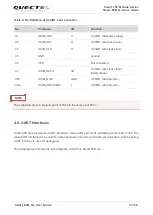
Table 9: Pin Definition of (U)SIM1 Card Connector
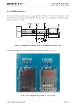
The schematic and pin assignment of J1002 are the same as
J1001’s.
UART Interfaces
4.9.
Smart EVB G2 provides two UART interfaces: main UART port J1301 and debug UART port J1302. The
main UART interface can be used for data transmission and AT command communication. And the debug
UART interface is used for debugging.
The following figure shows the block diagram of UART on Smart EVB G2.
No.
Pin Name
I/O
Function
C1
USIM_VDD
O
(U)SIM1 card power supply
C2
USIM_RST
O
(U)SIM1 card reset signal
C3
USIM_CLK
O
(U)SIM1 card clock signal
C5
GND
Ground
C6
VPP
Not connected
C7
USIM_DATA
I/O
(U)SIM1 card clock signal;
Bi-directional
CD1
USIM_GND
GND
(U)SIM1 card detection
CD2
USIM_PRESENCE
I
(U)SIM1 card detection
NOTE


