background image


GSM/GPRS/GNSS  Module  Series 

                                                                                                                            MC60  Series  Hardware  Design


MC60_Series_Hardware_Design                                Confidential / Released                                52 / 114 


VBAT

PWRKEY

(INPUT)

VDD_EXT 

(OUTPUT)

Logout from network in 2-12s

0.7s<Pulldown<1s

RUNNING

OFF

GSM PART STATUS


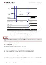
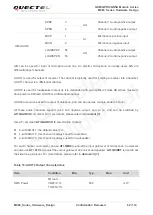
Figure 22: Turn-off Timing of GSM Part by Using the PWRKEY Pin 


3.8.2.2.  Power down GSM Part using Command 

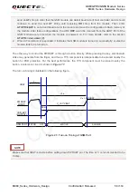
It is also a safe way to turn off the GSM module via AT command 

AT+QPOWD=1

. This command will let 

the GSM module log off from the network and allow the firmware to save important data before completely 

disconnecting the power supply. 


Before the completion of the power down procedure, the GSM module sends out the result code shown 

below: 


NORMAL POWER DOWN 


After that moment, no further AT commands can be executed. And then the GSM module enters into the 

power down mode.   


Please refer to 

document [1]

 for details about the AT command 

AT+QPOWD

.   


Quectel 

Confidential

Содержание MC60

Страница 1: ...MC60 Series Hardware Design GSM GPRS GNSS Module Series Rev MC60_Series_Hardware_Design_V2 0 Date 2017 05 15 www quectel com ...

Страница 2: ...S THE INFORMATION PROVIDED IS BASED UPON CUSTOMERS REQUIREMENTS QUECTEL MAKES EVERY EFFORT TO ENSURE THE QUALITY OF THE INFORMATION IT MAKES AVAILABLE QUECTEL DOES NOT MAKE ANY WARRANTY AS TO THE INFORMATION CONTAINED HEREIN AND DOES NOT ACCEPT ANY LIABILITY FOR ANY INJURY LOSS OR DAMAGE OF ANY KIND INCURRED BY USE OF OR RELIANCE UPON THE INFORMATION ALL INFORMATION SUPPLIED HEREIN IS SUBJECT TO C...

Страница 3: ...performance parameter in Table 38 1 3 2016 09 19 Tiger CHENG 1 Added the description of Periodic Mode Chapter 3 4 2 4 2 Added the description of AlwaysLocateTM mode Chapter 3 4 2 5 3 Added the description of GLP Mode Chapter 3 4 2 6 4 Added the description of PCM interface Chapter 3 9 5 Added the description of LOCUS Chapter 3 18 6 Added the current consumption data of BT function Table 44 2 0 201...

Страница 4: ... Drop 28 3 5 2 1 Decrease Supply Voltage Drop for GSM Part 28 3 5 2 2 Decrease Supply Voltage Drop for GNSS Part 29 3 5 3 Reference Design for Power Supply 30 3 5 3 1 Reference Design for Power Supply of GSM Part 30 3 5 3 2 Reference Design for Power Supply of GNSS part in All in one Solution 31 3 5 3 3 Reference Design for Power Supply of GNSS part in Stand alone Solution 31 3 5 4 Monitor Power S...

Страница 5: ...SM Part 51 3 8 2 1 Power down GSM Part Using the PWRKEY Pin 51 3 8 2 2 Power down GSM Part using Command 52 3 9 Serial Interfaces 53 3 9 1 UART Port 55 3 9 1 1 Features of UART Port 55 3 9 1 2 The Connection of UART 56 3 9 1 3 Firmware Upgrade 58 3 9 2 Debug Port 58 3 9 3 Auxiliary UART Port and GNSS UART Port 59 3 9 3 1 Connection in All in one Solution 59 3 9 3 2 Connection in Stand alone Soluti...

Страница 6: ...GNSS Antenna Interface 85 4 2 1 Antenna Specifications 85 4 2 2 Active Antenna 86 4 2 3 Passive Antenna 87 4 3 Bluetooth Antenna Interface 88 5 Electrical Reliability and Radio Characteristics 89 5 1 Absolute Maximum Ratings 89 5 2 Operating Temperature 90 5 3 Power Supply Ratings 90 5 4 Current Consumption 92 5 5 Electrostatic Discharge 95 6 Mechanical Dimensions 97 6 1 Mechanical Dimensions of M...

Страница 7: ...BLE 16 PIN DEFINITION OF THE UART INTERFACES 54 TABLE 17 PIN DEFINITION OF AUDIO INTERFACE 61 TABLE 18 AOUT2 OUTPUT CHARACTERISTICS 62 TABLE 19 TYPICAL ELECTRET MICROPHONE CHARACTERISTICS 66 TABLE 20 TYPICAL SPEAKER CHARACTERISTICS 66 TABLE 21 PIN DEFINITION OF PCM INTERFACE 67 TABLE 22 PCM PARAMETER CONFIGURATION 67 TABLE 23 AT QPCMON COMMAND PARAMETER CONFIGURATION 69 TABLE 24 AT QPCMVOL COMMAND...

Страница 8: ...F GSM PART GNSS IS POWERED OFF 92 TABLE 45 CURRENT CONSUMPTION OF GNSS PART 94 TABLE 46 BT CURRENT CONSUMPTION OF MC60 MODULE 94 TABLE 47 BT CURRENT CONSUMPTION OF MC60E MODULE 95 TABLE 48 ESD PERFORMANCE PARAMETER TEMPERATURE 25º C HUMIDITY 45 96 TABLE 49 REEL PACKAGING 104 TABLE 50 RELATED DOCUMENTS 105 TABLE 51 TERMS AND ABBREVIATIONS 106 TABLE 52 DESCRIPTION OF DIFFERENT CODING SCHEMES 112 TAB...

Страница 9: ...RN ON TIMING 46 FIGURE 19 TURN OFF TIMING BY USING THE PWRKEY PIN 47 FIGURE 20 TURN OFF TIMING OF GNSS PART BY USING AT COMMAND 48 FIGURE 21 TURN ON TIMING OF GSM PART 50 FIGURE 22 TURN OFF TIMING OF GSM PART BY USING THE PWRKEY PIN 52 FIGURE 23 REFERENCE DESIGN FOR FULL FUNCTION UART 56 FIGURE 24 REFERENCE DESIGN FOR UART PORT THREE LINE CONNECTION 57 FIGURE 25 REFERENCE DESIGN FOR UART PORT WITH...

Страница 10: ...TLIGHT 78 FIGURE 48 PPS VS NMEA TIMING 81 FIGURE 49 REFERENCE DESIGN FOR GSM ANTENNA 82 FIGURE 50 RF SOLDERING SAMPLE 85 FIGURE 51 REFERENCE DESIGN WITH ACTIVE ANTENNA 86 FIGURE 52 REFERENCE DESIGN WITH PASSIVE ANTENNA 87 FIGURE 53 REFERENCE DESIGN FOR BLUETOOTH ANTENNA 88 FIGURE 54 MC60 TOP AND SIDE DIMENSIONS UNIT MM 97 FIGURE 55 MC60 BOTTOM DIMENSIONS UNIT MM 98 FIGURE 56 RECOMMENDED FOOTPRINT ...

Страница 11: ...ng MC60 module Manufacturers of the cellular terminal should send the following safety information to users and operating personnel and incorporate these guidelines into all manuals supplied with the product If not so Quectel assumes no liability for the customer s failure to comply with these precautions Full attention must be given to driving at all times in order to reduce the risk of an accide...

Страница 12: ...d in a service area with adequate cellular signal strength Your cellular terminal or mobile contains a transmitter and receiver When it is ON it receives and transmits radio frequency energy RF interference can occur if it is used close to TV set radio computer or other electric equipment In locations with potentially explosive atmospheres obey all posted signs to turn off wireless devices such as...

Страница 13: ...consumption The embedded flash memory provides capacity for storing user specific configurations and allows for future updates MC60 is an SMD type module with 54 LCC pads and 14 LGA pads which can be easily embedded into applications With a compact profile of 18 7mm 16 0mm 2 1mm the module can meet almost all the requirements for M2M applications including vehicle and personal tracking wearable de...

Страница 14: ...ant to GSM Phase 2 2 GSM Class Small MS Transmitting Power Class 4 2W at GSM850 and EGSM900 Class 1 1W at DCS1800 and PCS1900 GPRS Connectivity GPRS multi slot class 12 default GPRS multi slot class 1 12 configurable GPRS mobile station class B DATA GPRS GPRS data downlink transfer max 85 6kbps GPRS data uplink transfer max 85 6kbps Coding scheme CS 1 CS 2 CS 3 and CS 4 Support the protocol PAP Pa...

Страница 15: ...0 06 80 Adaptive Multi Rate AMR Echo Suppression Noise Reduction Embedded one amplifier of class AB with maximum driving power up to 800mW UART Interfaces UART Port Seven lines on UART port interface Used for AT command and GPRS data Used for PMTK command and NMEA output in All in one solution Multiplexing function Support autobauding from 4800bps to 115200bps Debug Port Two lines on debug port in...

Страница 16: ...30dBm GPS Acquisition 29mA 130dBm GPS GLONASS Tracking 22mA 130dBm GPS GLONASS Standby 300uA VCC 3 3V Backup 14uA V_BCKP 3 3V Receiver Type GPS L1 1575 42MHz C A Code GLONASS L1 1598 0625 1605 375MHz C A Code Sensitivity GPS GLONASS Acquisition 149dBm Reacquisition 161dBm Tracking 167dBm Time to First Fix EASY Enabled 1 Cold Start 15s average 130dBm Warm Start 5s average 130dBm Hot Start 1s 130dBm...

Страница 17: ...dio frequency part Power management Peripheral interfaces Power supply Turn on off interface UART interface Audio interfaces U SIM interface Acceleration Accuracy Without aid 0 1m s Dynamic Performance Maximum Altitude 18000m Maximum Velocity 515m s Acceleration 4G GNSS UART Port GNSS UART port GNSS_TXD and GNSS_ RXD Support baud rate from 4800bps to 115200bps 115200bps by default Used for communi...

Страница 18: ...SAW GNSS_ANT GNSS_VCC_EN GNSS_VCC GNSS UART 32KHz AUDIO BT BT_ANT 26MHz TCXO RF Transceiver PMU VRTC Backup Domain MEMORY Serial Interface RF Part GNSS ADC 1PPS U SIM1 Interface U SIM2 Interface U SIM1 Interface Figure 1 Module Functional Diagram 2 4 Evaluation Board In order to help customers develop applications with MC60 Quectel supplies an evaluation board EVB TE A board RS 232 to USB cable po...

Страница 19: ...ing chapters provide detailed descriptions about these pins Pin of module Power supply Backup domain of GNSS Operating modes Power on down Power saving Serial interfaces Audio interfaces PCM interface U SIM card interface SD card interface ADC Behaviors of the RI Network status indication EASY autonomous AGPS technology EPO offline AGPS technology QuecFastFix Online technology Multi tone AIC LOCUS...

Страница 20: ...BAT UART MICN SPKP PWRKEY ADC SD_CMD SD_CLK SD_DATA SIM2_CLK SIM2_DATA SIM2_RST SIM_GND 1PPS SIM1_VDD SIM1_CLK SIM1_RST SIM1_DATA GNSS_TXD GNSS_RXD RXD_AUX TXD_AUX GNSS_VCC GND GNSS_VCC_EN DBG_TXD GND BT_ANT TXD RXD RI DCD DTR GND RESERVED NETLIGHT GND GND GND VBAT VBAT 55 RESERVED RESERVED 17 18 19 20 21 22 23 24 25 26 27 44 45 46 47 48 49 50 51 52 53 54 RESERVED RESERVED RESERVED RESERVED RESERV...

Страница 21: ...of GSM GPRS part VBAT 3 3V 4 6V VImax 4 6V VImin 3 3V VInorm 4 0V It must be able to provide sufficient current up to 1 6A in a transmitting burst GNSS_ VCC 26 PI Power supply of GNSS part GNSS_VCC 2 8V 4 3V VImax 4 3V VImin 2 8V VInorm 3 3V Assure load current no less than 150mA VRTC 52 IO Power supply for GNSS s backup domain Charging for backup battery or golden capacitor when the VBAT is appli...

Страница 22: ...down for a moment to turn on or turn off the system VILmax 0 1 VBAT VIHmin 0 6 VBAT VIHmax 3 1V Audio Interface Pin Name Pin No I O Description DC Characteristics Comment MICP MICN 1 2 AI Positive and negative voice input Refer to Chapter 3 10 6 If unused keep these pins open SPKP SPKN 3 4 AO Channel 1 positive and negative voice output 1 If unused keep these pins open 2 Support both voice and rin...

Страница 23: ... used for communication it is recommended to keep all other pins open RXD 34 DI Receive data DTR 37 DI Data terminal ready RI 35 DO Ring indication DCD 36 DO Data carrier detection CTS 38 DO Clear to send RTS 39 DI Request to send Debug Port Pin Name Pin No I O Description DC Characteristics Comment DBG_ TXD 29 DO Transmit data The same as UART port If unused keep these pins open DBG_ RXD 30 DI Re...

Страница 24: ...pad to U SIM card connector SIM1_ CLK SIM2_ CLK 19 10 DO Clock signal of U SIM card VOLmax 0 15 SIM_VDD VOHmin 0 85 SIM_VDD SIM1_ DATA SIM2_ DATA 21 11 IO Data signal of U SIM card VILmax 0 25 SIM_VDD VIHmin 0 75 SIM_VDD VOLmax 0 15 SIM_VDD VOHmin 0 85 SIM_VDD SIM1_ RST SIM2_ RST 20 12 DO Reset signal of U SIM card VOLmax 0 15 SIM_VDD VOHmin 0 85 SIM_VDD SIM_ GND 16 Specified ground for U SIM card...

Страница 25: ...MD 7 DO Command signal of SD card VILmin 0V VILmax 0 25 VDD_EXT VIHmin 0 75 VDD_EXT VIHmax VDD_EXT 0 2 VOHmin 0 85 VDD_EXT VOLmax 0 15 VDD_EXT If unused keep these pins open SD_CLK 8 DO Clock signal of SD card SD_DATA 9 IO Data signal of SD card Antenna Interface Pin Name Pin No I O Description DC Characteristics Comment RF_ ANT 41 IO GSM antenna pad Impedance of 50Ω BT_ ANT 32 IO BT antenna pad I...

Страница 26: ...cation between GSM and GNSS parts such as AT command sending for GNSS control GNSS part firmware upgrading and EPO data download In Stand alone solution GSM and GNSS parts work independently and thus have to be controlled separately All in one solution and Stand alone solution schematic diagrams are shown below 2 Keep this pin open in Stand alone solution 1PPS 17 DO One pulse per second VOLmax 0 4...

Страница 27: ...UART_AUX GNSS_UART GNSS_VCC GNSS_VCC_EN LDO EN OUT IN LDO VBAT DC 5V PWRKEY VRTC BACKUP DOMAIN PWRKEY VBAT MCU Figure 3 All in one Solution Schematic Diagram MC60 UART PORT GNSS_UART PORT MCU GNSS_VCC LDO DC 5V LDO PWRKEY EN VBAT VRTC BACKUP DOMAIN VBAT PWRKEY Figure 4 Stand alone Solution Schematic Diagram Quectel Confidential ...
Страница 28: ...s recommended that the maximum voltage drop during the burst transmission does not exceed 400mV All in one Stand alone Remarks Firmware upgrade Firmware upgrade via UART Port GSM and GNSS parts share the same firmware package Firmware upgrade via UART Port GSM and GNSS parts share the same firmware package Refer to Chapter 3 9 1 3 for details Data transmission Both GSM and GNSS data are transmitte...

Страница 29: ...ly Voltage Drop for GSM Part Power supply range of the GSM part is from 3 3V to 4 6V Make sure that the input voltage will never drop below 3 3V even in a burst transmission If the power voltage drops below 3 3V the module will be turned off automatically For better power performance it is recommended to place a 100uF tantalum capacitor with low ESR ESR 0 7Ω and ceramic capacitors 100nF 33pF and 1...

Страница 30: ...art Power supply range of GNSS part is from 2 8 to 4 3V GNSS_VCC s maximum average current is 40mA during GNSS acquisition after power up So it is important to supply sufficient current and make the power clean and stable The decouple combination of 10uF and 100nF capacitor is recommended nearby GNSS_VCC pin A reference circuit is illustrated in the following figure GNSS_VCC C2 C1 GND 10uF 100nF F...

Страница 31: ... is recommended to be used as the power supply The following figure shows a reference design for 5V input power source for GSM part The designed output for the power supply is 4 0V and the maximum load current is 3A In addition in order to get a stable output voltage a zener diode is placed close to the pins of VBAT As to the zener diode it is suggested to use a zener diode whose reverse zener vol...

Страница 32: ...ics of GNSS_VCC_EN to match LDO s EN pin Please refer to document 1 for details about the AT commands for GNSS control VBAT C1 C2 SGM2019 ADJYN5G TR U1 VIN VOUT 1 5 4 7uF 100nF R1 75K 1 43K 1 R2 1uF 2 3 C3 4 EN FB GND GNSS_VCC GNSS_VCC_EN Module 26 28 U2 47K R3 Figure 9 Reference Circuit Design for GNSS part in All in one Solution 3 5 3 3 Reference Design for Power Supply of GNSS part in Stand alo...

Страница 33: ...omain which contains all the necessary GNSS information for quick start up and a small amount of user configuration variables In GNSS s backup mode the backup domain is still alive As long as the backup domain is alive EASY technology will be available 3 5 5 1 Use VBAT as the Backup Power Source of GNSS In either All in one or Stand alone solution GNSS s backup mode will be active as long as the m...

Страница 34: ... is turned off and GNSS_VCC is also powered off a backup supply such as a coin cell battery rechargeable or non chargeable or a super capacitor can be used to power the VRTC pin to keep GNSS in backup mode In this case the current consumption is as low as 14uA approximately When powered by VRTC the reference schematic diagrams in All in one and Stand alone solutions are shown below Rechargeable Ba...

Страница 35: ... powered for the longest time in all system power supplies 3 6 Operating Modes 3 6 1 Operating Modes of GSM Part The table below briefly summarizes the various operating modes of GSM part mentioned in the following chapters Table 9 Operating Modes Overview of GSM Part Modes Function GSM Normal Operation GSM GPRS Sleep After enabling Sleep mode by AT QSCLK 1 the GSM part will automatically enter in...

Страница 36: ...PCL dynamic DTX control and the working RF band GPRS IDLE The GSM part is not registered on GPRS network It is not reachable through GPRS channel GPRS STANDBY The GSM part is registered on GPRS network but no GPRS PDP context is active The SGSN knows the Routing Area where the module is located at GPRS READY The PDP context is active but no data transfer is ongoing The GSM part is ready to receive...

Страница 37: ...ault setting is AT QSCLK 0 and in this mode the GSM part cannot enter Sleep mode When the GSM part is set by the command AT QSCLK 1 customers can control the part to enter into or exit from the Sleep mode through pin DTR When DTR is set to high level and there is no on air or hardware interrupt such as GPIO interrupt or data on UART port the GSM part will enter into Sleep mode automatically In thi...

Страница 38: ...Table 10 Default Configuration of Full on Mode GNSS part Item Configuration Comment Baud Rate 115200bps Protocol NMEA RMC VTG GGA GSA GSV and GLL Update Rate 1Hz SBAS Enable AIC Enable LOCUS Disable EASY Technology Enable EASY will be disabled automatically when update rate exceeds 1Hz GNSS GPS GLONASS In full on mode the consumption complies with the following regulations When the GNSS part is po...

Страница 39: ...ot or Warm start The typical current consumption is about 300uA GNSS_VCC 3 3V in standby mode Sending the following PMTK command can make GNSS part enter into standby mode PMTK161 0 28 send this command in Stand alone solution The following methods will make GNSS part exit from standby mode Sending any data via GNSS_UART will make GNSS part exit from standby mode in Stand alone solution Standby mo...

Страница 40: ...wn below Table 11 Format of the PMTK Command Enabling Periodic Mode Format PMTK225 Type Run_time Sleep_time 2nd_run_time 2nd_sleep_time checksum CR LF Parameter Format Description Range ms Type Decimal Type 1 Periodic backup mode Type 2 Periodic standby mode Run_time Decimal Run_time Full on mode period ms 1000 518400 000 Sleep_time Decimal Sleep_time Standby Backup mode period ms 1000 518400000 2...

Страница 41: ...the module is in tracking mode otherwise the module may have a risk of failure in satellite tracking If module is located in weak signal areas it is better to set a longer 2nd_run_time to ensure the success of reacquisition Power Run time Run time Sleep time Sleep time Second run time Second run time Second sleep time Second sleep time Run time Run time Sleep time Sleep time Full on Figure 14 Oper...

Страница 42: ...ll make the module back to full on mode AlwaysLocateTM backup mode is similar to AlwaysLocateTM standby mode The difference is that the AlwaysLocateTM backup mode allows the module to switch automatically between full on mode and backup mode Sending PMTK225 9 22 command will make the module enter into AlwaysLocateTM backup mode During the Full on mode period in AlwaysLocateTM backup mode sending P...

Страница 43: ...Consumption in GLP Mode and Normal Mode Scenario In GLP Mode mA In Normal Mode mA Static 8 9 22 Walking 11 2 22 Running 11 5 22 Driving 21 5 22 Customers can use the following commands to make the module enter into or exit from the GLP mode PQGLP W 1 1 21 The command is used to set the module into GLP mode When PQGLP W OK 09 is returned it means the module has entered into GLP mode successfully PQ...

Страница 44: ...in Stand alone Solution GSM Part Modes GNSS Part Modes Full on Standby Backup Normal Sleep Minimum Functionality 1 The mark means that the Part supports this mode 2 In All in one solution all PMTK commands used for the GNSS part should be sent through the GSM UART after the GNSS part is powered on Make sure the GSM UART Port is accessible 3 In All in one solution when the GSM part is in Sleep mode...

Страница 45: ...ase refer to document 14 MC60E module adopts dual mode chip and supports BT3 0 BT4 0 specifications BT4 0 supports Bluetooth low power BLE technology which is low cost short range and interoperable wireless technology and uses intelligent means to minimize power consumption thus extends the applicability of the technology to a wide range of extended applications such as watch anti theft key ring s...

Страница 46: ... UART Port of the module every time when the module is powered on For more details refer to the section AT IPR in document 1 2 When AT command is responded it indicates the module is turned on successfully or else the module fails to be turned on The other way to control the PWRKEY is through a button directly While pressing the key electrostatic strike may generate from the finger and thus a TVS ...

Страница 47: ...own PWRKEY pin The time of T1 is recommended to be 100ms 3 7 2 Power down The following procedures can be used to turn off the module Normal power down procedure Turn off module using the PWRKEY pin Normal power down procedure Turn off module using command AT QPOWD Under voltage automatic shutdown Take effect when under voltage is detected 3 7 2 1 Power down Module Using the PWRKEY Pin It is a saf...

Страница 48: ...hen autobauding is active and DTE DCE are not correctly synchronized after start up the module is recommended to be set to a fixed baud rate 2 As network logout time is related to the local mobile network it is recommended to delay about 12 seconds before disconnecting the power supply or restarting the module After that moment no further AT commands can be executed Then the module enters the powe...

Страница 49: ...s out the result code shown below NORMAL POWER DOWN After that moment no further AT commands can be executed And then the module enters into the power down mode Please refer to document 1 for details about the AT command AT QPOWD 3 7 2 3 Power down GNSS part Alone Using AT Command It is a safe way to turn off the GNSS part alone via AT command AT QGNSSC 0 The power down scenario for GNSS part is i...

Страница 50: ...ended to be set to a fixed baud rate 3 8 Power on and down Scenarios in Stand alone Solution In Stand alone solution GSM and GNSS parts are controlled separately and thus the power on and down control of them are independent from each other as well The GSM part can be turned on off or restarted via PWRKEY pin control which is the same as that in All in one solution The GNSS part is turned on off v...

Страница 51: ...1 2 When AT command is responded it indicates the GSM module is turned on successfully or else the module fails to be turned on The other way to control the PWRKEY is through a button directly While pressing the key electrostatic strike may generate from the finger and thus a TVS component is indispensable to be placed nearby the button for ESD protection For the best performance the TVS component...

Страница 52: ...as the following figure The power down procedure causes the GSM module to log off from the network and allows the firmware to save important data before completely disconnecting the power supply Before the completion of the power down procedure the GSM module sends out the result code shown below NORMAL POWER DOWN 1 When unsolicited result codes do not appear when autobauding is active and DTE DCE...

Страница 53: ...fe way to turn off the GSM module via AT command AT QPOWD 1 This command will let the GSM module log off from the network and allow the firmware to save important data before completely disconnecting the power supply Before the completion of the power down procedure the GSM module sends out the result code shown below NORMAL POWER DOWN After that moment no further AT commands can be executed And t...

Страница 54: ...e module up RI Ring indicator when there is a call SMS or URC output the module will inform DTE with the RI pin DCD Data carrier detection the validity of this pin demonstrates successful set up of the communication link The Debug Port DBG_TXD Send data to the COM port of peripheral DBG_RXD Receive data from the COM port of peripheral The Auxiliary UART Port In All in one solution TXD_AUX Send dat...

Страница 55: ... 2 V VOL 0 0 15 VDD_EXT V VOH 0 85 VDD_EXT VDD_EXT V Interface Pin Name Pin No I O Description UART Port TXD 33 DO Transmit data RXD 34 DI Receive data DTR 37 DI Data terminal ready RI 35 DO Ring indication DCD 36 DO Data carrier detection CTS 38 DO Clear to send RTS 39 DI Request to send Debug Port DBG_RXD 30 DI Receive data DBG_TXD 29 DO Transmit data Auxiliary UART Port 1 RXD_AUX 1 24 DI Receiv...

Страница 56: ... 2 2 is used to enable hardware flow control AT command AT IFC 0 0 is used to disable the hardware flow control For more details please refer to document 1 After setting a fixed baud rate or autobauding please send AT string at that rate The UART port is ready when it responds OK Autobauding allows the module to detect the baud rate by receiving the string AT or at from the host or PC automaticall...

Страница 57: ...auding from a fixed baud rate If autobauding is active it is not recommended to switch to multiplex mode To assure reliable communication and avoid any problems caused by undetermined baud rate between DCE and DTE it is strongly recommended to configure a fixed baud rate and save it instead of using autobauding after start up For more details please refer to the Section AT IPR in document 1 3 9 1 ...

Страница 58: ...E Host DTE Controller Figure 24 Reference Design for UART Port Three Line Connection A reference design for UART Port with hardware flow control is shown as below The connection will enhance the reliability of the mass data communication RTS CTS RTS CTS GND RXD TXD TXD RXD GND Module DCE Host DTE Controller Figure 25 Reference Design for UART Port with Hardware Flow Control Quectel Confidential ...
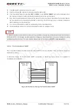
Страница 59: ...Reference Design for Firmware Upgrade 1 In Stand alone solution make sure the Auxiliary UART Port is connected to the GNSS UART Port during firmware upgrade Please refer to Chapter 3 9 3 2 for details 2 The firmware of module might need to be upgraded due to a certain reasons It is thus recommended to reserve these pins in the host board for firmware upgrade 3 9 2 Debug Port Two lines DBG_TXD and ...

Страница 60: ...ection in All in one Solution As the GNSS part of MC60 outputs more data than a single GNSS system the default output NMEA types running in 4800bps baud rate and 1Hz update rate will lose some data The solution to avoid losing data in 4800bps baud rate and 1Hz update rate is to decrease the output NMEA types 115200bps baud rate is enough to transmit GNSS NMEA in default settings and it is thus rec...

Страница 61: ...ystem please change the 5 6K resistors to 10K ones Peripheral TXD RXD 1K TXD RXD RTS CTS DTR RI RTS CTS GPIO EINT GPIO DCD Module 1K 1K 5 6K 5 6K 5 6K 1K 1K 1K 1K GND GND Voltage level 3 3V Figure 30 Level Match Design for 3 3V System It is highly recommended to add the resistor divider circuit on the UART signal lines when the host s level is 3V or 3 3V For a higher voltage level system a level s...

Страница 62: ...3V T1IN T2IN T3IN T4IN R1IN R2IN R3IN R1OUT R2OUT R3OUT T1OUT T2OUT T5OUT T3OUT T4OUT T5IN GND GND R1OUT 1 2 3 4 5 6 7 8 9 GND To PC Serial Port GND 1K 1K 1K 1K 1K 5 6K 5 6K 1K 1K 5 6K RS 232 Level Shifter Figure 31 Sketch Map for RS 232 Interface Match Please visit vendors websites to select a suitable IC such as http www maximintegrated com and http www exar com 3 10 Audio Interfaces The module ...

Страница 63: ... by AT QAUDCH command For more details please refer to document 1 Use AT command AT QAUDCH to select audio channel 0 AIN AOUT1 the default value is 0 1 AIN AOUT2 this channel is always used for earphone 2 AIN AOUT2 this channel is always used for loudspeaker For each channel customers can use AT QMIC to adjust the input gain level of microphone Customers can also use AT CLVL to adjust the output g...

Страница 64: ...1800 TDD noise is more obvious Therefore customers can have a choice based on test results Sometimes even no RF filtering capacitor is required The capacitor which is used for filtering out RF noise should be close to the audio interface Audio alignment should be as short as possible In order to decrease radio or other signal interference the position of RF antenna should be kept away from audio i...

Страница 65: ...0pF 0603 33pF 0603 Figure 33 Handset Interface Design for AOUT1 SPKP SPKN Differential layout Amplifier circuit Module 10pF 0603 Close to speaker GND ESD 33pF 0603 33pF 0603 GND 10pF 0603 ESD 10pF 0603 33pF 0603 Figure 34 Speaker Interface Design with an Amplifier for AOUT1 A suitable differential audio amplifier can be chosen from the Texas Instrument s website http www ti com There are also othe...

Страница 66: ...lose to Module GND 33pF 33pF Differential layout 33pF MICN 0603 0603 0603 0603 0603 0603 0603 10pF GND 10pF 0603 0603 0603 10pF 10pF Figure 35 Earphone Interface Design 3 10 5 Loud Speaker Interface Design LOUDSPKN 0R 0R LOUDSPKP 8 ohm Module GND GND GND Close to Speaker 10pF 33pF 33pF 10pF 10pF 33pF GND GND GND Differential layout 0603 0603 0603 0603 0603 0603 ESD ESD Figure 36 Loud Speaker Inter...

Страница 67: ...er Min Typ Max Unit Working Voltage 1 2 1 5 2 0 V Working Current 200 500 uA External Microphone Load Resistance 2 2 Kohm Parameter Min Typ Max Unit AOUT1 Output Single ended Load resistance 32 Ohm Reference level 0 2 4 Vpp Differential Load resistance 32 Ohm Reference level 0 4 8 Vpp AOUT2 Output Differential Load resistance 8 Ohm Reference level 0 2 VBAT Vpp Single ended Load resistance 8 Ohm Re...

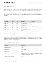
Страница 68: ...6 bit linear code PCM format through software configuration The sample rate is 8KHz and the clock source rate is 256KHz The module can only act in master mode The PCM interface supports both long and short frame synchronization and it only supports MSB first For more detailed information please refer to the table below Table 22 PCM Parameter Configuration Pin Name Pin No I O Description Comment PC...

Страница 69: ...on formats 12 11 10 9 8 7 6 5 4 3 2 1 0 12 11 10 9 8 7 6 5 4 3 2 1 0 PCM_CLK PCM_SYNC PCM_OUT PCM_IN MSB MSB 13 14 15 15 0 15 0 13 14 15 14 14 1 1 Figure 37 Timing Diagram for Long Frame Synchronization PCM_CLK PCM_SYNC PCM_OUT PCM_IN 12 11 10 9 8 7 6 5 4 3 2 1 0 12 11 10 9 8 7 6 5 4 3 2 1 0 MSB MSB 13 14 15 13 14 15 0 15 15 1 1 0 14 14 Figure 38 Timing Diagram for Short Frame Synchronization PCM ...

Страница 70: ... for the configuration of PCM AT QPCMON and AT QPCMVOL Details are illustrated below AT QPCMON is used to configure the operating mode of PCM Command format AT QPCMON mode Sync_Type Sync_Length SignExtension MSBFirst Table 23 AT QPCMON Command Parameter Configuration Parameter Value Range Description Mode 0 2 0 Close PCM 2 Open PCM when audio talk is set up Sync_Type 0 1 0 Short frame synchronizat...

Страница 71: ...supported Table 25 Pin Definition of U SIM Card Interface Parameter Value Range Description vol_pcm_in 0 32767 Set the input volume vol_pcm_out 0 32767 Set the output volume The voice may be distorted when this value exceeds 16384 Pin Name Pin No I O Description Alternate Function 1 SIM1_VDD 18 PO Supply power for U SIM1 card Automatic detection of U SIM1 card voltage Voltage accuracy 3 0V 5 and 1...

Страница 72: ... SIM1 card interface with an 8 pin U SIM card connector VDD_EXT Module 22R 22R 22R 10K 100nF GND GND TVS 33pF 33pF 33pF 33pF VCC RST CLK IO VPP GND GND U SIM Card Connector SIM_GND SIM1_VDD SIM1_RST SIM1_CLK SIM1_PRESENCE SIM1_DATA Figure 40 Reference Circuit for U SIM1 Card Interface with an 8 Pin U SIM Card Connector Maximum supply current is around 10mA SIM2_CLK 10 DO Clock signal of U SIM2 car...

Страница 73: ...gure 41 Reference Circuit for U SIM1 Card Interface with a 6 Pin U SIM Card Connector The following figure shows a reference design for U SIM2 card interface with a 6 pin U SIM card connector Module 22R 22R 22R 100nF GND TVS 33pF 33pF 33pF VCC RST CLK IO VPP GND GND 33pF U SIM Card Connector SIM_GND SIM2_VDD SIM2_RST SIM2_CLK SIM2_DATA Figure 42 Reference Circuit for U SIM2 Card Interface with a 6...

Страница 74: ...protection Please note that the U SIM peripheral circuit should be close to the U SIM card connector The pull up resistor on SIM_DATA line can improve anti jamming capability when long layout trace and sensitive occasion are applied and should be placed close to the U SIM card connector 3 13 SD Card Interface The module provides an SD card interface that supports many types of memory such as Memor...

Страница 75: ...1 VDD CLK VSS2 47K 47K 47K 4 7uF 0 1nF VDD_EXT 33R 33R 33R 1 2 3 4 5 6 7 8 9 SD card connector Figure 43 Reference Circuit for SD Card Interface Table 27 Pin Definition of SD Card and T Flash Micro SD Card SD_DATA 9 IO Data signal of SD card Pin No Pin Name of SD Card Pin Name of T Flash Micro SD Card 1 CD DATA3 DATA2 2 CMD CD DATA3 3 VSS1 CMD 4 VDD VDD 5 CLK CLK 6 VSS2 VSS 7 DATA0 DATA0 8 DATA1 D...

Страница 76: ...more than 50pF and should be placed as close as possible to the SD card connector Reserve external pull up resistors for other data lines except the DATA0 signal The SD_CLK and SD_DATA traces are recommended to be shielded by ground in order to improve EMI suppression capability and prevent the crosstalk 3 14 ADC The module provides an ADC channel to measure the value of voltage Please give priori...

Страница 77: ...RI Behavior as a Receiver When Voice Calling State RI Response Standby HIGH Voice Call Change to LOW and then Change to HIGH when call is established Change to HIGH when use ATH to hang up the call Change to HIGH first when calling part hangs up and then change to LOW for 120ms indicating NO CARRIER as an URC After that RI changes to HIGH again Change to HIGH when SMS is received SMS When a new SM...

Страница 78: ...S Received 3 16 Network Status Indication The NETLIGHT signal can be used to drive a network status indicator LED The working state of this pin is listed in the following table Table 31 Working State of the NETLIGHT State Module Function Off The module is not running 64ms On 800ms Off The module is not synchronized with network 64ms On 2 000ms Off The module is synchronized with network 64ms On 60...

Страница 79: ... orbit information automatically up to 3 days after first receiving the broadcast ephemeris and save the predicted information into the internal memory GNSS part of MC60 will use the information for positioning if no enough information from satellites so the function is helpful for positioning and TTFF improvement The EASY function can reduce TTFF to 5s in warm start In this case GNSS s backup dom...

Страница 80: ...o document 14 Make sure the EPO function is enabled if customers need to download the EPO data 3 19 QuecFastFix Online Technology QuecFastFix Online function can be used in combination with EPO technology to further improve TTFF and acquisition sensitivity in cold start Based on the latest EPO data QuecFastFix Online additionally offers adding information such as reference location and NITZ NTP ti...

Страница 81: ...rovides a log capacity of more than 16 hours The detail procedures of this function are illustrated below The module has fixed the position only effective in 3D_fixed scenario Sending PMTK command PMTK184 1 22 to erase internal flash Sending PMTK command PMTK185 0 22 to start logging The module logs the basic information UTC time latitude longitude and height every 15 seconds to internal flash mem...

Страница 82: ...0 UTC 12 00 01 PPS Figure 48 PPS VS NMEA Timing The feature only supports 1Hz NMEA output and baud rate at 14400bps 115200bps When the baud rate is 9600bps or 4800bps it only supports RMC NMEA sentence output Because at low baud rates per second transmission may exceed one second if there are many NMEA sentences output Customers can enable this function by sending PMTK255 1 2D and disable the func...

Страница 83: ...na pad The RF interface of the three antenna pads has an impedance of 50Ω 4 1 GSM Antenna Interface There is a GSM antenna pad named RF_ANT for MC60 Table 32 Pin Definition of the RF_ANT 4 1 1 Reference Design The external antenna must be matched properly to achieve the best performance so the matching circuit is necessary A reference design for GSM antenna is shown below Module RF_ANT 0R NM NM Fi...

Страница 84: ... be used to adjust the RF performance To minimize the loss on RF trace and RF cable please pay attention to the design The following table shows the requirement on GSM antenna Table 33 Antenna Cable Requirements Type Requirements GSM850 EGSM900 Cable insertion loss 1dB DCS1800 PCS1900 Cable insertion loss 1 5dB Table 34 Antenna Requirements Type Requirements Frequency Range Depend on the frequency...

Страница 85: ...3 RF Receiving Sensitivity Table 36 RF Receiving Sensitivity 4 1 4 Operating Frequencies Table 37 Operating Frequencies PCS1900 30dBm 2dB 0dBm 5dB Frequency Receive Sensitivity GSM850 110dBm EGSM900 110dBm DCS1800 110dBm PCS1900 110dBm Frequency Receive Transmit ARFCH GSM850 869MHz 894MHz 824MHz 849MHz 128 251 EGSM900 925MHz 960MHz 880MHz 915MHz 0 124 975 1023 DCS1800 1805MHz 1880MHz 1710MHz 1785M...

Страница 86: ...tems The RF signal is obtained from the GNSS_ANT pin The impedance of RF trace should be controlled as 50Ω and the trace length should be kept as short as possible 4 2 1 Antenna Specifications The module can be connected to a dedicated GPS GLONASS passive or active antenna to receive GPS GLONASS satellite signals The recommended antenna specifications are given in the following table Table 38 Reco...

Страница 87: ...s 0Ω The external active antenna is powered by GNSS_VCC The voltage ranges from 2 8V to 4 3V and the typical value is 3 3V If the voltage does not meet the requirements for powering the active antenna an external LDO should be used The inductor L1 is used to prevent the RF signal from leaking into the GNSS_VCC pin and route the bias supply to the active antenna and the recommended value of L1 is n...

Страница 88: ...enna Module Passive Antenna GNSS_ANT C1 NM C2 NM R1 П matching circuit 0R Figure 52 Reference Design with Passive Antenna The above figure is a typical reference design with passive antenna C1 R1 and C2 are reserved matching circuit for antenna impedance modification C1 and C2 are not mounted by default R1 is 0Ω Impedance of RF trace should be controlled as 50Ω and the trace length should be kept ...

Страница 89: ... the matching circuit is necessary The connection is recommended as the following figure Module BT_ANT 0R NM NM Figure 53 Reference Design for Bluetooth Antenna There are some suggestions for component placement and RF trace layout for Bluetooth RF traces Antenna matching circuit should be closed to the antenna The impedance of RF trace should be controlled as 50Ω The RF traces should be kept far ...

Страница 90: ...y and voltage on digital and analog pins of the module are listed in the following table Table 40 Absolute Maximum Ratings Parameter Min Max Unit VBAT 0 3 4 73 V GNSS_VCC 0 3 4 5 V Peak Current of Power Supply VBAT 0 2 A RMS Current of Power Supply VBAT during one TDMA frame 0 0 7 A Voltage at Digital Pins 0 3 3 08 V Voltage at Analog Pins 0 3 3 08 V Voltage at Digital analog Pins in Power Down Mo...

Страница 91: ...might reduce in their value and exceed the specified tolerances When the temperature returns to the normal operating temperature levels the module will meet 3GPP specifications again 5 3 Power Supply Ratings Table 42 Power Supply Ratings of GSM Part GNSS is Powered off Parameter Min Typ Max Unit Operation temperature range 1 35 25 75 Extended temperature range 2 40 85 Parameter Description Conditi...

Страница 92: ... 1 Peak supply current VCC 3 3V 150 mA VRTC Backup domain voltage supply 1 5 2 8 3 3 V Sleep mode AT CFUN 4 IDLE mode Sleep mode 0 68 13 0 73 mA mA mA TALK mode GSM850 EGSM900 1 DCS1800 PCS1900 2 208 209 142 146 mA mA DATA mode GPRS 3Rx 2Tx GSM850 EGSM900 1 DCS1800 PCS1900 2 359 360 232 250 mA mA DATA mode GPRS 2 Rx 3Tx GSM850 EGSM900 1 DCS1800 PCS1900 2 431 413 311 339 mA mA DATA mode GPRS 4 Rx 1...

Страница 93: ...83mA power level 19 Typical 63mA DCS1800 power level 0 250mA Typical 153mA power level 7 Typical 73mA power level 15 Typical 60mA PCS1900 power level 0 250mA Typical 151mA power level 7 Typical 76mA power level 15 Typical 61mA GPRS Data DATA Mode GPRS 3 Rx 2Tx CLASS 12 GSM850 power level 5 550mA Typical 363mA power level 12 Typical 131mA power level 19 Typical 91mA EGSM900 power level 5 550mA Typi...

Страница 94: ...al 216mA power level 12 Typical 103mA power level 19 Typical 83mA EGSM900 power level 5 350mA Typical 222mA power level 12 Typical 104mA power level 19 Typical 84mA DCS1800 power level 0 300mA Typical 171mA power level 7 Typical 96mA power level 15 Typical 82mA PCS1900 power level 0 300mA Typical 169mA power level 7 Typical 98mA power level 15 Typical 83mA DATA Mode GPRS 1 Rx 4Tx CLASS 12 GSM850 p...

Страница 95: ...Typ Unit IVCC Acquisition VCC 3 3V GPS 25 mA IVCC Tracking VCC 3 3V GPS 19 mA IVCC Acquisition VCC 3 3V GPS GLONASS 29 mA IVCC Tracking VCC 3 3V GPS GLONASS 22 mA IVCC Standby VCC 3 3V 0 3 mA IBCKP backup V_BCKP 3 3V 14 uA The tracking current is tested in following conditions For Cold Start 10 minutes after First Fix For Hot Start 15 seconds after First Fix Table 46 BT Current Consumption of MC60...

Страница 96: ...should still be emphasized Proper ESD handling and packaging procedures must be applied throughout the processing handling and operation of any applications using the module The measured ESD values of the module are shown in the following table RF State GSM State BT State Current Consumption Full function AT CFUN 1 IDLE Off Advertising 13 01mA 13 59mA SLEEP Off Advertising 1 42mA 2 06mA Disable fr...

Страница 97: ...s_Hardware_Design Confidential Released 96 114 Table 48 ESD Performance Parameter Temperature 25º C Humidity 45 Test Point Contact Discharge Air Discharge VBAT GND 5KV 10KV RF_ANT 5KV 10KV TXD RXD 2KV 4KV GNSS_TXD GNSS_RXD 2KV 4KV Others 0 5KV 1KV Quectel Confidential ...
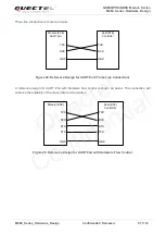
Страница 98: ...sign MC60_Series_Hardware_Design Confidential Released 97 114 6 Mechanical Dimensions This chapter describes the mechanical dimensions of the module 6 1 Mechanical Dimensions of Module Figure 54 MC60 Top and Side Dimensions Unit mm Quectel Confidential ...

Страница 99: ...eries_Hardware_Design Confidential Released 98 114 Figure 55 MC60 Bottom Dimensions Unit mm The two arc test points in the above recommended footprint should be treated as keepout areas keepout means do not pour copper on the mother board NOTE Quectel Confidential ...

Страница 100: ...60_Series_Hardware_Design Confidential Released 99 114 6 2 Recommended Footprint Figure 56 Recommended Footprint Unit mm For easy maintenance of the module please keep about 3mm between the module and other components in the host PCB NOTE Quectel Confidential ...
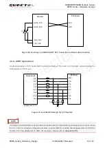
Страница 101: ...eased 100 114 6 3 Top and Bottom Views of the Module Figure 57 Top Views of MC60 and MC60E Figure 58 Bottom Views of MC60 and MC60E These are design effect drawings of MC60 and MC60E modules For more accurate pictures please refer to the module that customers get from Quectel NOTE Quectel Confidential ...
Страница 102: ...d at 10 RH 3 Devices require baking before mounting if any circumstance below occurs When the ambient temperature is 23º C 5º C and the humidity indication card shows the humidity is 10 before opening the vacuum sealed bag Device mounting cannot be finished within 72 hours when the ambient temperature is 30º C and the humidity is 60 Stored at 10 RH 4 If baking is required devices should be baked f...

Страница 103: ...low temperature is from 235º C to 245º C for SnAg3 0Cu0 5 alloy The absolute maximum reflow temperature is 260º C To avoid damage to the module caused by repeated heating it is suggested that the module should be mounted after reflow soldering for the other side of PCB has been completed Recommended reflow soldering thermal profile is shown below Time 50 100 150 200 250 300 50 100 150 200 250 160º...

Страница 104: ... Released 103 114 7 3 Packaging MC60 is packaged in a vacuum sealed bag which is ESD protected The bag should not be opened until the devices are ready to be soldered onto the application The following figures show the packaging details measured in mm Figure 60 Tape Dimensions Quectel Confidential ...
Страница 105: ...esign Confidential Released 104 114 Figure 61 Reel Dimensions Table 49 Reel Packaging Model Name MOQ for MP Minimum Package 250pcs Minimum Package x 4 1000pcs MC60 250pcs Size 370mm 350mm 56mm N W 0 32kg G W 1 08kg Size 380mm 250mm 365mm N W 1 28kg G W 4 8kg Quectel Confidential ...

Страница 106: ...nications Phase 2 Use of Data Terminal Equipment Data Circuit terminating Equipment DTE DCE interface for Short Message Service SMS and Cell Broadcast Service CBS 6 GSM 11 14 Digital cellular telecommunications Phase 2 Specification of the U SIM Application Toolkit for the Subscriber Identity module Mobile Equipment U SIM ME interface 7 GSM 11 11 Digital cellular telecommunications Phase 2 Specifi...

Страница 107: ...IO application note 14 Quectel_MC60_GNSS_AGPS_Application_Note MC60 GNSS AGPS application note 15 Quectel_GSM_BT_Application_Note GSM BT application note Abbreviation Description ADC Analog to Digital Converter AG Audio Gateway AGPS Assisted GPS AIC Active Interference Cancellation AIN Audio In AMR Adaptive Multi Rate ARP Antenna Reference Point ASIC Application Specific Integrated Circuit BER Bit...

Страница 108: ...d Full Rate EGSM Enhanced GSM EMC Electromagnetic Compatibility EPO Extended Prediction Orbit ESD Electrostatic Discharge ETS European Telecommunication Standard FCC Federal Communications Commission U S FDMA Frequency Division Multiple Access FR Full Rate FS File System FTP File Transfer Protocol GAGAN GPS Aided Geo Augmented Navigation GGA NMEA Global Positioning System Fix Data GLL NMEA Geograp...

Страница 109: ...nds free Profile HR Half Rate HTTP Hypertext Transfer Protocol I O Input Output IC Integrated Circuit IEEE Institute of Electrical and Electronics Engineers IMEI International Mobile Equipment Identity IOmax Maximum Output Load Current kbps Kilo Bits Per Second LCC Leadless Chip Carriers LED Light Emitting Diode LGA Land Grid Array Li Ion Lithium Ion MCU Micro Control Unit MMS Microsoft Media Serv...

Страница 110: ...ket Switched Broadcast Control Channel PCB Printed Circuit Board PCL Power Control Level PCM Pulse Code Modulation PDP Packet Data Protocol PDU Protocol Data Unit PING Packet Internet Groper PMOS Positive Channel Metal Oxide Semiconductor PMTK MTK Proprietary Protocol PMU Power Management Unit PPP Point to Point Protocol PPS Pulse per Second QZSS Quasi Zenith Satellite System RF Radio Frequency RM...

Страница 111: ...col TDMA Time Division Multiple Access TE Terminal Equipment 3GPP 3rd Generation Partnership Project TTFF Time to First Fix TX Transmitting Direction UART Universal Asynchronous Receiver Transmitter UDP User Datagram Protocol URC Unsolicited Result Code USIM Universal Mobile Telecommunication System USSD Unstructured Supplementary Service Data VSWR Voltage Standing Wave Ratio VTG NMEA Track Made G...

Страница 112: ...Imin Absolute Minimum Input Voltage Value VOHmax Maximum Output High Level Voltage Value VOHmin Minimum Output High Level Voltage Value VOLmax Maximum Output Low Level Voltage Value VOLmin Minimum Output Low Level Voltage Value WAAS Wide Area Augmentation System Phonebook Abbreviations LD U SIM Last Dialing phonebook list of numbers most recently dialed MC Mobile Equipment list of unanswered MT Ca...

Страница 113: ...ferent Coding Schemes Scheme Code Rate USF Pre coded USF Radio Block excl USF and BCS BCS Tail Coded Bits Punctured Bits Data Rate Kb s CS 1 1 2 3 3 181 40 4 456 0 9 05 CS 2 2 3 3 6 268 16 4 588 132 13 4 CS 3 3 4 3 6 312 16 4 676 220 15 6 CS 4 1 3 12 428 16 456 21 4 Radio block structure of CS 1 CS 2 and CS 3 is shown as the figure below Figure 62 Radio Block Structure of CS 1 CS 2 and CS 3 Rate 1...

Страница 114: ...dware Design MC60_Series_Hardware_Design Confidential Released 113 114 Radio block structure of CS 4 is shown as the following figure Figure 63 Radio Block Structure of CS 4 Block Code No coding 456 bits USF BCS Radio Block Quectel Confidential ...
Страница 115: ...Written as 3 1 or 2 2 the first number indicates the amount of downlink timeslots while the second number indicates the amount of uplink timeslots The active slots determine the total number of slots the GPRS device can use simultaneously for both uplink and downlink communications The description of different multi slot classes is shown in the following table Table 53 GPRS Multi slot Classes Mult...

Отзывы: