background image

Reference Design

A

MC60

Tiger CHENG

CHECKED BY

DRAWN BY

OF

A

6

5

4

3

2

1

SHEET

A

B

C

D

1

2

3

4

5

6

D

C

B

Quectel Wireless Solutions

PROJECT

SIZE

TITLE

VER

6

6

DATE

2016/5/30

A2

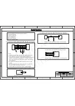
VOHmin=0.85*VDD_EXT
VOLmax=0.15*VDD_EXT
VILmax=0.25*VDD_EXT
VIHmin=0.75*VDD_EXT

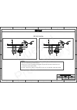
Connection of All Functional UART Port for 3.3V System

1. CTS&RTS will be used for HW flow control when mass data has been sent.

2. When AT+QSCLK=1 is set on the module, customer's application can 

control the module to enter into or exit from the sleep mode through the pin DTR.
When DTR is set to high level, and there is no on-air or hardware interrupt,
such as GPIO interrupt or data on serial port, the module will enter into sleep 

3. RI will output an indication signal when activity such as voice call  or SMS

NOTES

VDD_EXT=2.8V (typical value)

Electric characteristics of the module's input and output port: 

MC60

4. DCD is mainly applied in modem communication (PPP). The active status

represents the communication link has been set up.

5. Please pay attention to the level match of UART in product application.

Connection of Three-line UART Port for 3.3V System

MC60

Please pay attention to the level match of UART in product application.

MCU/ARM

mode automatically.

is coming.

VIHmax=0.2V

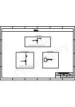
It is recommended to reserve the points for upgrading the firmware. 

Serial Interface

MC60

MC60

It is recommended to reserve the points for debug port. 

Please pay attention to the level match of UART in product application.

1

TXD

2

RXD

3

RTS

4

CTS

5

GPIO

6

EINT

7

GPIO

8

GND

MCU/ARM

R608

1K

R604

1K

R605

1K

R606

1K

R607

1K

R609

1K

R610

1K

R601

1K

R602

1K

1

TXD

2

RXD

3

GND

R612

5K6

R611

5K6

R613

5K6

R603

5K6

1

T607

1

T608

1

T601

1

T602

1

T603

1

T605

1

T606

1

T604

[1,6]

RXD

[1,6]

TXD

[1]

RTS

[1]

CTS

[1]

DTR

[1]

RI

[1]

DCD

[1,6]

RXD

[1,6]

TXD

[1]

DBG_RXD

[1]

DBG_TXD

[1,5]

PWRKEY

VBAT

[1,6]

RXD

[1,6]

TXD

VCC_3V3

Quectel 

Preliminary

Содержание MC60

Страница 1: ...MC60 Reference Design GSM GPRS GNSS Module Series Rev A Date 2016 05 30 www quectel com...

Страница 2: ...FORMATION PROVIDED IS BASED UPON CUSTOMERS REQUIREMENTS QUECTEL MAKES EVERY EFFORT TO ENSURE THE QUALITY OF THE INFORMATION IT MAKES AVAILABLE QUECTEL DOES NOT MAKE ANY WARRANTY AS TO THE INFORMATION...

Страница 3: ...PRS GNSS Module Series MC60 Reference Design MC60_Reference_Design Confidential Released 2 4 About the Document History Revision Date Author Description A 2016 05 30 Tiger CHENG Initial Quectel Prelim...

Страница 4: ...RS GNSS Module Series MC60 Reference Design MC60_Reference_Design Confidential Released 3 4 Contents About the Document 2 Contents 3 1 Introduction 4 1 1 Introduction 4 1 2 Schematics 4 Quectel Prelim...

Страница 5: ...Design Confidential Released 4 4 1 Introduction 1 1 Introduction This document is a reference design for MC60 module The schematics included in this document are preliminary and are subject to change...

Страница 6: ...e Antenna Power Supply Circuit AntennaType Active Passive Need No need MC60 module does not support PCM BT SD card function NOTE B101 XH414 C101 NM_Golden capacitor R104 R106 C103 1uF C105 33pF C102 4...

Страница 7: ...vehicle application eg DC12V IN DCDC DC 5V OUT LDO DC 4V OUT FOR 2 Use DCDC to convert high input voltage to 5V and LDO will generate 4V 3 3V typical voltage for the module DC input Power Supply NOTE...

Страница 8: ...n Close to Speaker 4 AOUT1 is capable of driving 32ohm load 5 AOUT2 is capable of driving 8ohm load and Earphone Note 1 4 1 3 2 J303 HANDSETCON C322 33pF C327 10pF C328 33pF C329 10pF C330 33pF C314 3...

Страница 9: ...d to be routed to the Pin 16 SIM_GND of the module separately It should be placed nearby SIM card holder Note1 Note2 Note3 SIM Card Note1 Note2 Note3 R403 22R R405 22R R407 22R C401 100nF 1 2 3 4 5 6...

Страница 10: ...TE 2016 5 30 Reference Design MC60 A2 LED Indication Pin NETLIGHT indicates the network status Driver Recommended circuit for turning on off the module Turn on off MCU MCU GPIO R501 1K D501 1 GPIO 2 G...

Страница 11: ...of the module s input and output port MC60 4 DCD is mainly applied in modem communication PPP The active status represents the communication link has been set up 5 Please pay attention to the level ma...

Отзывы: