background image


GSM/GPRS  Module  Series 

                                                                                                                                M85  Hardware  Design


M85_Hardware_Design                                  Confidential / Released                                                  60 / 88   


Table 19: Pin Definition of the ADC 


Table 20: Characteristics of the ADC 


3.13.  Behaviors Of The RI 

Table 21: Behaviors of the RI 


If URC of SMS is disabled, the RI will not change.


Pin Name   

Pin No. 

Description 

ADC0 

Analog to digital converter. 

Item 

Min. 

Typ. 

Max. 

Units 

Voltage Range 


2.8 

ADC Resolution 


10 


bits 

ADC Accuracy 


2.7 


mV 

State 

RI response   

Standby 

HIGH 

Voice Calling 

Change to LOW, then: 

1.    Change to HIGH when call is established. 

2.    Use ATH to hang up the call, RI changes to HIGH. 

3.    Calling  part  hangs  up,  RI  changes  to  HIGH  first,  and  changes  to  LOW  for 


120ms indicating ―NO CARRIER‖ as an URC, then changes to HIGH again. 

4.    Change to HIGH when SMS is received. 

SMS 

When a new SMS comes, the RI changes to LOW and holds low level for about 120 

ms, then changes to HIGH. 

URC 

Certain URCs can trigger 120ms low level on RI.   

NOTE 

Содержание M85

Страница 1: ...M85 Hardware Design GSM GPRS Module Series Rev M85_Hardware_Design_V3 0 Date 2015 10 22 www quectel com...

Страница 2: ...NFORMATION PROVIDED IS BASED UPON CUSTOMERS REQUIREMENTS QUECTEL MAKES EVERY EFFORT TO ENSURE THE QUALITY OF THE INFORMATION IT MAKES AVAILABLE QUECTEL DOES NOT MAKE ANY WARRANTY AS TO THE INFORMATION...

Страница 3: ...03 13 Stone YU Hollis WANG 1 Updated module key features in Table 1 2 Modified pin assignment in Figure 2 3 Updated DC characteristics of module s pins in Table 4 4 Updated reference circuit for powe...

Страница 4: ...t 17 3 1 2 Pin Description 18 3 2 Operating Modes 23 3 3 Power Supply 24 3 3 1 Power Features of Module 24 3 3 2 Decrease Supply Voltage Drop 24 3 3 3 Reference Design For Power Supply 25 3 3 4 Monito...

Страница 5: ...Card Interfaces 50 3 10 SD Card Interface 53 3 11 PCM Interface 55 3 11 1 Configuration 56 3 11 2 Timing 56 3 11 3 Reference Design 58 3 11 4 AT Command 58 3 12 ADC 59 3 13 Behaviors Of The RI 60 3 1...

Страница 6: ...ware_Design Confidential Released 5 88 6 4 Bottom View of the Module 77 7 Storage and Manufacturing 78 7 1 Storage 78 7 2 Soldering 79 7 3 Packaging 80 8 Appendix A Reference 82 9 Appendix B GPRS Codi...

Страница 7: ...INTERFACE 55 TABLE 16 CONFIGURATION 56 TABLE 17 QPCMON COMMAND DESCRIPTION 59 TABLE 18 QPCMVOL COMMAND DESCRIPTION 59 TABLE 19 PIN DEFINITION OF THE ADC 60 TABLE 20 CHARACTERISTICS OF THE ADC 60 TABL...

Страница 8: ...EFERENCE DESIGN FOR FIRMWARE UPGRADE 41 FIGURE 21 REFERENCE DESIGN FOR DEBUG PORT 41 FIGURE 22 REFERENCE DESIGN FOR AUXILIARY UART PORT 42 FIGURE 23 LEVEL MATCH DESIGN FOR 3 3V SYSTEM 42 FIGURE 24 SKE...

Страница 9: ...RF SOLDERING SAMPLE 67 FIGURE 48 M85 MODULE TOP AND SIDE DIMENSIONS UNIT MM 74 FIGURE 49 M85 MODULE BOTTOM DIMENSIONS UNIT MM 75 FIGURE 50 THE PAD DIMENSIONS UNIT MM 75 FIGURE 51 RECOMMENDED FOOTPRINT...

Страница 10: ...and describes its hardware interface which are connected with the customer application and the air interface This document can help you quickly understand module interface specifications electrical a...

Страница 11: ...s devices on boarding the aircraft If your device offers a Flight Mode which must be enabled prior to boarding an aircraft Switch off your wireless device when in hospitals or clinics or other health...

Страница 12: ...ontrol etc M85 is an SMD type module with LCC package which can be easily embedded into applications It provides abundant hardware interfaces like PCM and SD Card Interface Designed with power saving...

Страница 13: ...such as PDA uses M85 module the device needs to do permissive change and SAR testing The following list indicates the performance of antenna gain in certificate testing 2 3 Key Features The following...

Страница 14: ...eration 40 C 35 C and 80 C 85 C 1 Storage temperature 45 C 90 C SMS Text and PDU mode SMS storage SIM card SIM Interfaces Support SIM card 1 8V 3V Audio Features Speech codec modes Half Rate ETS 06 20...

Страница 15: ...s the major functional parts Radio frequency part Serial Flash Power management The Peripheral interface Power supply Turn on off interface UART interfaces Audio interfaces SIM interfaces SD interface...

Страница 16: ...tus Netlight UART SIM Interfaces Reset ESD PMU MEMORY Audio Audio PCM Interface PCM Serial Flash SD Interface SD ADC ADC Figure 1 Module Functional Diagram 2 5 Evaluation Board In order to help custom...

Страница 17: ...3 Application Interface The module adopts LCC package and has 83 pins The following chapters provide detailed descriptions about these pins below Power supply Power on down Power saving RTC Serial in...

Страница 18: ...8 29 30 31 32 33 34 35 36 37 38 39 40 41 42 43 44 45 46 47 48 49 50 51 52 53 54 55 56 57 58 59 60 61 62 63 64 65 66 67 68 69 70 71 72 73 74 Top view RF SIM2 VBAT UART ADC0 RESERVED SPK2P AGND MIC2P MI...

Страница 19: ...tery or golden capacitor when the VBAT is applied VImax 3 3V VImin 1 5V VInorm 2 8V VOmax 3V VOmin 2V VOnorm 2 8V Iout max 2mA Iin 10uA If unused keep this pin open VDD_EXT 60 O Supply 2 8V voltage fo...

Страница 20: ...urns on while output low level when module turns off VOHmin 0 85 VDD_EXT VOLmax 0 15 VDD_EXT If unused keep this pin open Audio Interface PIN NAME PIN NO I O DESCRIPTION DC CHARACTERISTICS COMMENT MIC...

Страница 21: ...15 VDD_EXT If only use TXD RXD and GND to communicate recommended connecting RTS to GND via 0R resistor and keeping other pins open RXD 50 I Receive data TXD 49 O Transmit data RTS 51 I Request to se...

Страница 22: ...ILmax 0 25 SIM_VDD VIHmin 0 75 SIM_VDD VOLmax 0 15 SIM_VDD VOHmin 0 85 SIM_VDD SIM2_DATA 73 SIM1_RST 53 O SIM reset VOLmax 0 15 SIM_VDD VOHmin 0 85 SIM_VDD SIM2_RST 74 SIM1_ PRESENCE 57 I SIM card det...

Страница 23: ...CRIPTION DC CHARACTERISTICS COMMENT SD_CMD 34 O SD command VILmin 0V VILmax 0 25 VDD_EXT VIHmin 0 75 VDD_EXT VIHmax VDD_EXT 0 2 VOHmin 0 85 VDD_EXT VOLmax 0 15 VDD_EXT If unused keep these pins open S...

Страница 24: ...rough GPRS channel GPRS STANDBY The module is registered to GPRS network but no GPRS PDP context is active The SGSN knows the Routing Area where the module is located at GPRS READY The PDP context is...

Страница 25: ...AT In order to ensure stable operation of the module it is recommended that the max voltage drop during the transmit burst does not exceed 400mV Vdrop 4 615ms 577us IBAT VBAT Burst 1 6A Figure 3 Volta...

Страница 26: ...power supply If there is a big voltage difference between the input source and the desired output VBAT a switcher power converter is recommended to use as a power supply Figure 5 shows a reference de...

Страница 27: ...w level voltage An open collector driver circuit is suggested to control the PWRKEY A simple reference circuit is illustrated as below Turn on pulse PWRKEY 4 7K 47K Figure 6 Turn on the Module with an...

Страница 28: ...WRKEY is through a button directly A TVS component is indispensable to be placed nearby the button for ESD protection For the best performance the TVS component must be placed nearby the button When p...

Страница 29: ...dule using command AT QPOWD Over voltage or under voltage automatic shutdown Take effect when over voltage or under voltage is detected Emergent power down procedure Turn off module using the EMERG_OF...

Страница 30: ...ng the module 3 For more details about the application of STATUS pin please refer to the Chapter 3 15 3 4 2 2 Power Down Module Using AT Command It is also a safe way to turn off the module via AT com...

Страница 31: ...ower down mode and only RTC is still active 1 These unsolicited result codes do not appear when autobauding is active and DTE and DCE are not correctly synchronized after start up The module is recomm...

Страница 32: ...t could cause destroying of the code or data area of the flash memory in the module Therefore it is recommended that PWRKEY or AT command should always be the preferential way to turn off the system 3...

Страница 33: ...onality mode and DTR hardware interface signal can be used to lead system to SLEEP mode 3 5 1 Minimum Functionality Mode Minimum functionality mode reduces the functionality of the module to a minimum...

Страница 34: ...enter or exit from the SLEEP mode through pin DTR When DTR is set to high level and there is no on air or hardware interrupt such as GPIO interrupt or data on UART port the module will enter SLEEP mod...

Страница 35: ...the main power supply VBAT is removed after the module is turned off a backup supply such as a coin cell battery rechargeable or non chargeable or a super cap can be used to supply the VRTC pin to kee...

Страница 36: ...35 88 Non chargeable Backup Battery Module RTC Core VBAT Power Supply LDO DCDC LDO VRTC 1 5K Figure 14 VRTC is Supplied by a Non chargeable Battery Rechargeable Backup Battery Module RTC Core VBAT Pow...

Страница 37: ...rovides three serial ports UART Port Debug Port and Auxiliary Port The module is designed as a DCE Data Communication Equipment following the traditional DCE DTE Data Terminal Equipment connection Aut...

Страница 38: ...end data to the COM port of computer DBG_RXD Receive data from the COM port of computer The Auxiliary UART Port TXD_AUX Send data to the RXD of DTE RXD_AUX Receive data from the TXD of DTE The logic l...

Страница 39: ...le hardware flow control After setting a fixed baud rate or autobauding please send AT string at that rate The UART port is ready when it responds OK Autobauding allows the module to detect the baud r...

Страница 40: ...ay receive unknown characters after switching to new baud rate It is not recommended to switch to autobauding from a fixed baud rate If autobauding is active it is not recommended to switch to multipl...

Страница 41: ...rt UART Port with hardware flow control is shown as below This connection will enhance the reliability of the mass data communication RTS CTS RTS CTS GND RXD TXD TXD RXD GND Module DCE Host DTE Contro...

Страница 42: ...e upgraded due to certain reasons It is recommended to reserve these pins in the host board for firmware upgrade 3 7 2 Debug Port Two lines DBG_TXD and DBG_RXD It outputs log information automatically...

Страница 43: ...QEAUART 1 string on the UART port The default baud rate setting is 115200bps and does not support autobauding The baud rate can be modified by AT QSEDCB command For more details please refer to the d...

Страница 44: ...RS 232 interface Since the electrical level of module is 2 8V so a RS 232 level shifter must be used Note that you should assure the IO voltage of level shifter which connects to module is 2 8V TXD R...

Страница 45: ...t of receiver which can be used as a single ended channel SPK2P and AGND can establish a pseudo differential mode AOUT3 is used for loud speaker output as it embedded an amplifier of class AB whose ma...

Страница 46: ...u would have to discuss with its capacitor vendor to choose the most suitable capacitor for filtering out GSM850MHz EGSM900MHz DCS1800MHz and PCS1900MHz separately The severity degree of the RF interf...

Страница 47: ...following figure MICxP Differential layout Module 10pF 33pF 33pF 33pF GND GND Electret Microphone GND GND 10pF 10pF GND GND ESD ESD MICxN Close to Microphone 0603 0603 0603 0603 0603 0603 Figure 25 Re...

Страница 48: ...yout Amplifier circuit Module 10pF 0603 Close to speaker GND ESD 33pF 0603 33pF 0603 GND 10pF 0603 ESD 10pF 0603 33pF 0603 Figure 27 Speaker Interface Design with an Amplifier for AOUT1 SPK2P AGND Dif...

Страница 49: ...T2 The suitable differential audio amplifier can be chosen from the Texas Instrument s website http www ti com There are other excellent audio amplifier vendors in the market too 4 The value of C1 and...

Страница 50: ...603 0603 Figure 31 Loud Speaker Interface Design 3 8 6 Audio Characteristics Table 10 Typical Electret Microphone Characteristics Table 11 Typical Speaker Characteristics Parameter Min Typ Max Unit Wo...

Страница 51: ...ecification and also supports the functionality of the new GSM Phase 2 specification for FAST 64 kbps SIM card which is intended for use with a SIM application Tool kit The SIM interface is powered by...

Страница 52: ...tion function is disabled Your application can use AT QSIMDET 1 0 and AT QSIMDET 0 0 to switch on and off the SIM card detection function For details of this AT command please refer to document 1 When...

Страница 53: ...Holder GND TVS 33pF33pF 33pF VCC RST CLK IO VPP GND GND 33pF Figure 33 Reference Circuit for SIM1 Interface with the 6 pin SIM Card Holder The following figure is the reference design for SIM2 interfa...

Страница 54: ...ted will go through the ESD device first and then lead to module The 22 resistors should be connected in series between the module and the SIM card so as to suppress the EMI spurious transmission and...

Страница 55: ..._EXT 33R 33R 33R SD Socket 1 2 3 4 5 6 7 8 9 Figure 35 Reference Circuit for SD Card Table 14 Pin Definition of the SD Card Interface Pin Name Pin No Description SD_CMD 34 Command signal of SD card ou...

Страница 56: ...ls with the capacitance less than 15pF Reserve external pull up resistors for other data lines except the DATA0 signal The SD_CLK and SD_DATA0 line must be shielded by ground in order to improve EMI 3...

Страница 57: ...alid The following diagram shows the timing of different combinations The synchronization length in long synchronization format can be programmed by firmware from one bit to eight bits In the Sign ext...

Страница 58: ...on Figure 36 Long Synchronization Sign Extension Diagram 12 11 10 9 8 7 6 5 4 3 2 1 0 12 11 10 9 8 7 6 5 4 3 2 1 0 PCM_CLK PCM_SYNC PCM_OUT PCM_IN MSB MSB Zero padding Zero padding Figure 37 Long Sync...

Страница 59: ...3 11 3 Reference Design M85 can only work as a master providing synchronization and clock source The reference design is shown as below PCM_SYNC PCM_CLK PCM_OUT PCM_IN PCM_SYNC PCM_CLK PCM_IN PCM_OUT...

Страница 60: ...on ADC0 pin For details of this AT command please refer to the document 1 In order to improve the accuracy of ADC the layout of ADC should be surrounded by ground Parameter Scope Description Mode 0 2...

Страница 61: ...ltage Range 0 2 8 V ADC Resolution 10 bits ADC Accuracy 2 7 mV State RI response Standby HIGH Voice Calling Change to LOW then 1 Change to HIGH when call is established 2 Use ATH to hang up the call R...

Страница 62: ...On the other hand when it is used as a receiver the timing of the RI is shown as below RI Idle Ring Off hook by ATA On hook by ATH SMSreceived HIGH LOW Figure 41 RI Behavior of Voice Calling as a Rec...

Страница 63: ...or NETLIGHT 3 15 Operating Status Indication The STATUS pin will output a high level after the module being turned on but it is not recommended connecting this pin to a MCU s GPIO to judge whether the...

Страница 64: ...Design M85_Hardware_Design Confidential Released 63 88 Table 23 Pin Definition of the STATUS Module 300R 4 7K 47K VBAT STATUS Figure 45 Reference Design for STATUS Pin Name Pin No Description STATUS...

Страница 65: ...24 Pin Definition of the RF_ANT 4 1 Reference Design The external antenna must be matched properly to achieve best performance so the matching circuit is necessary the reference design for RF is shown...

Страница 66: ...g Besides a type match circuit is suggested to be used to adjust the RF performance 4 2 RF Output Power Table 25 The Module Conducted RF Output Power In GPRS 4 slots TX mode the max output power is re...

Страница 67: ...e Requirements GSM850 EGSM900 Cable insertion loss 1dB DCS1800 PCS1900 Cable insertion loss 1 5dB Table 29 Antenna Requirements Type Requirements Frequency Range GSM850 EGSM900 DCS1800 PCS1900MHz VSWR...

Страница 68: ...5_Hardware_Design Confidential Released 67 88 4 6 RF Cable Soldering Soldering the RF cable to RF pad of module correctly will reduce the loss on the path of RF please refer to the following example o...

Страница 69: ...for power supply and voltage on digital and analog pins of module are listed in the following table Table 30 Absolute Maximum Ratings Parameter Min Max Unit VBAT 0 3 4 73 V Peak current of power suppl...

Страница 70: ...Supply Ratings Table 32 The Module Power Supply Ratings Parameter Min Typ Max Unit Normal Temperature 35 25 80 Restricted Operation1 40 35 80 85 Storage Temperature 45 90 Parameter Description Condit...

Страница 71: ...13 1 0 mA mA TALK mode GSM850 EGSM9001 DCS1800 PCS19002 223 219 153 151 mA mA DATA mode GPRS 3Rx 2Tx GSM850 EGSM9001 DCS1800 PCS19002 363 393 268 257 mA mA DATA mode GPRS 2Rx 3Tx GSM850 EGSM9001 DCS1...

Страница 72: ...Typical 91mA EGSM900 power level 5 550mA Typical 393mA power level 12 Typical 132mA power level 19 Typical 92mA DCS1800 power level 0 450mA Typical 268mA power level 7 Typical 112mA power level 15 Typ...

Страница 73: ...vel 5 350mA Typical 216mA power level 12 Typical 103mA power level 19 Typical 83mA EGSM900 power level 5 350mA Typical 233mA power level 12 Typical 104mA power level 19 Typical 84mA DCS1800 power leve...

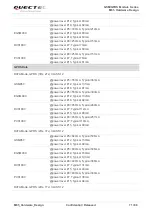
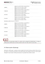
Страница 74: ...Confidential Released 73 88 The measured ESD values of module are shown as the following table Table 34 The ESD Endurance Temperature 25 C Humidity 45 Tested Point Contact Discharge Air Discharge VBAT...

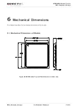
Страница 75: ...re Design M85_Hardware_Design Confidential Released 74 88 6 Mechanical Dimensions This chapter describes the mechanical dimensions of the module 6 1 Mechanical Dimensions of Module Figure 48 M85 Modul...

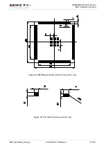
Страница 76: ...GSM GPRS Module Series M85 Hardware Design M85_Hardware_Design Confidential Released 75 88 Figure 49 M85 Module Bottom Dimensions Unit mm Figure 50 The PAD Dimensions Unit mm...

Страница 77: ...ies M85 Hardware Design M85_Hardware_Design Confidential Released 76 88 6 2 Recommended Footprint Figure 51 Recommended Footprint Unit mm The module should keep about 3mm away from other components in...

Страница 78: ...Module Series M85 Hardware Design M85_Hardware_Design Confidential Released 77 88 6 3 Top View of the Module Figure 52 Top View of the Module 6 4 Bottom View of the Module Figure 53 Bottom View of th...

Страница 79: ...ent of 30 C temperature and 60 RH Stored at 10 RH Devices require baking before mounting if any circumstance below occurs When the ambient temperature is 23 C 5 C humidity indication card shows the hu...

Страница 80: ...of the module pads should be 0 2 mm for M85 For more details please refer to document 13 It is suggested that peak reflow temperature is from 235 C to 245 C for SnAg3 0Cu0 5 alloy Absolute max reflow...

Страница 81: ...form The reel is 330mm in diameter and each reel contains 250pcs modules This is especially suitable for the M85 according to SMT assembly processes requirements The tape is packed in a vacuum sealed...

Страница 82: ...ntial Released 81 88 DC 44 PS 6 DETAIL A DETAIL A Figure 55 Tape and Reel Information Table 35 Reel Packing Model Name MOQ for MP Minimum Package 250pcs Minimum Package 4 1000pcs M85 250pcs Size 370 3...

Страница 83: ...ent DTE DCE interface for Short Message Service SMS and Cell Broadcast Service CBS 6 GSM 11 14 Digital cellular telecommunications Phase 2 Specification of the SIM Application Toolkit for the Subscrib...

Страница 84: ...eference Point ASIC Application Specific Integrated Circuit BER Bit Error Rate BOM Bill Of Material BTS Base Transceiver Station CHAP Challenge Handshake Authentication Protocol CS Coding Scheme CSD C...

Страница 85: ...ate GMSK Gaussian Minimum Shift Keying GPRS General Packet Radio Service GSM Global System for Mobile Communications G W Gross Weight HR Half Rate I O Input Output IC Integrated Circuit IMEI Internati...

Страница 86: ...er Identification Module SMS Short Message Service TDMA Time Division Multiple Access TE Terminal Equipment TX Transmitting Direction UART Universal Asynchronous Receiver Transmitter URC Unsolicited R...

Страница 87: ...vel Voltage Value VOHmin Minimum Output High Level Voltage Value VOLmax Maximum Output Low Level Voltage Value VOLmin Minimum Output Low Level Voltage Value Phonebook Abbreviations LD SIM Last Dialing...

Страница 88: ...ent Coding Schemes Scheme Code Rate USF Pre coded USF Radio Block excl USF and BCS BCS Tail Coded Bits Punctured Bits Data Rate Kb s CS 1 1 2 3 3 181 40 4 456 0 9 05 CS 2 2 3 3 6 268 16 4 588 132 13 4...

Страница 89: ...M85 Hardware Design M85_Hardware_Design Confidential Released 88 88 Radio block structure of CS 4 is shown as the following figure Figure 57 Radio Block Structure of CS 4 Block Code No coding 456 bit...

Страница 90: ...tten as 3 1 or 2 2 the first number indicates the amount of downlink timeslots while the second number indicates the amount of uplink timeslots The active slots determine the total number of slots the...

Отзывы: